Maker Pro
Maker Pro

Designing a Converter!

sid2286

Aug 24, 2011
102
Joined
Aug 24, 2011
Messages
102
Hi,

I am trying to design a current to voltage converter (4mA to 20mA input and 0 to 1V output)but my problem is I want to have a multiple inputs and multiple outputs.
for eg. I have 8 analog current input and want 8 corresponding voltage output.

so far what I have designed is as follows:

1. Get the input (current) with shunt resistor converter to voltage, give it to ADC read from ADC into microcontroller, give back to DAC and get desired output.

So should I repeat this 8 times for 8 inputs or is there a better way other than this.

please recommend!

Thanks,
Sid
 

Harald Kapp

Moderator
Moderator
Nov 17, 2011
13,747
Joined
Nov 17, 2011
Messages
13,747
So should I repeat this 8 times for 8 inputs or is there a better way other than this.
Why A/D and D/A? Use a 62.5 Ohm resistor for each channel. 20mA*62.5Ohm=1.25V
Add an OpAmp as buffer and use it to subtract 250mV. This will result in:
4mA -> 250mV (across the resistor) -> 0V (output of the buffer)
20mA -> 1.25V (across the resistor) -> 1V (output of the buffer)

Of course you can use an ADC/µC and DAC, but that would be cracking a nut with a sledgehammer.
 

sid2286

Aug 24, 2011
102
Joined
Aug 24, 2011
Messages
102
Oh wonderful! thanks,

As recommended by you I designed a basic circuit, can you please check and let me know if that is correct or any modifications are required. ?

Thanks,
Sid
 

Attachments

  • ckt1.pdf
    16.5 KB · Views: 146

Harald Kapp

Moderator
Moderator
Nov 17, 2011
13,747
Joined
Nov 17, 2011
Messages
13,747
In general, your circuit should work.

In my view it is still too complex:

1) Why do you use a difference amplifier for U1A? The negative input is always at 0V (gnd). Therefore a simple voltage follower would suffice.

2) Why do you use U1a at all? You can bypass U1a and connect R11 directly to R1. The voltage at R1 is equal to the voltage at the output of U1A (gain=1). Foregoing U1A saves you 8 OpAmps, 2 chips and lots of passive components.

3) Why do you use the OPA07? The OPA07 requires a negative supply. If you use the MCP604 instead, you have only 2 ICs instead of 8. Plus the MCP604 is rail-to rail at the output, and input includes GND. This will allow you to operate the MCP604 from +5V only, sparing you the inverter U3 and the complete negative supply rail.#

By the way: when you use a single supply, you will not be able to discern current <4mA. Any current <4mA (or no current at all) will generate 0V at the output of the OpAmp. If you need an indication for this range of currents, use a dual supply. Any current <4mA will show up as a negative voltage at the output of the OpAmp.
 
Last edited:

sid2286

Aug 24, 2011
102
Joined
Aug 24, 2011
Messages
102
Thanks Harald Kapp,

I modified the circuit and it seems very basic circuit but please have a look and suggest if its fine or not, or any more further modifications are required.

Thanks
Sid
 

Attachments

  • CKT2.pdf
    13.3 KB · Views: 174

sid2286

Aug 24, 2011
102
Joined
Aug 24, 2011
Messages
102
Thanks Harald Kapp,

However I have a question, using the above circuit the output will come to exact 0v or will there be any offsets., ? how do I read from the IC datasheet? like what section to refer to?
 

Harald Kapp

Moderator
Moderator
Nov 17, 2011
13,747
Joined
Nov 17, 2011
Messages
13,747
The datasheet states "Rail-to-Rail Output" in the "features" section (page 1).

Table "DC characteristics" maximum output swing characterizes this in more detail as Vss+15mV for Rl=25kOhm (with output overdrive -> non-linear) or Vss+100mV for Rl=25kOhm (linear).
If this offset is an issue for your appplicatin, you will need the negative suply.
 

sid2286

Aug 24, 2011
102
Joined
Aug 24, 2011
Messages
102
ok so this means that the output in normal condition varies from rail to rail, however incase of 25kohm load, the offset will be of 100mV. Am I correct with my understanding?
 

Harald Kapp

Moderator
Moderator
Nov 17, 2011
13,747
Joined
Nov 17, 2011
Messages
13,747
25k is a small load. It is in the physics of the output transistors that there is a small voltage drop, even if the OpAmp is designated as rail-to-rail. The voltage drop will be smaller, if the current is smaller (load resistance is higher), But it will almost never reach exactly 0V.
That's the point where you need the negative supply.
 

sid2286

Aug 24, 2011
102
Joined
Aug 24, 2011
Messages
102
Hi assembled the given circuit on general purpose board, since I didnt had the 62.5E resistor I used a trimpot to get the required value.

rest of the circuit is as it is using MCP601 instead of MCP604. and taking the input (4-20mA) converting it into voltage using the pot, and giving it to non inverting terminal.

then I set the 250mV value on invertering terminal.

But I doubt if its working as a substractor.

the reading what I observed are as follows:

4mA signal. voltage at Pin6 of MCP601 is 0v., it remains constant till current is 7mA.

then suddenly it raising and at 8mA the opamp goes into saturation (5V).

I havent used any capacitor yet.

Please suggest what is wrong.

Thanks
Sid
 

Harald Kapp

Moderator
Moderator
Nov 17, 2011
13,747
Joined
Nov 17, 2011
Messages
13,747
Sounds correct, unless your actual setup deviates from your description. A quick simulation using LTSPICE and a universal opamp model confirms this.

Check:
- what is the voltage across the 62.5Ohm resistor?
- are all 410k resistors in place and connected correctly? You cannot connect either of the voltages dirctly to any of the opamp inputs.
- do you have dual supply? Add bypasss capacitors for bettter stability.
 

sid2286

Aug 24, 2011
102
Joined
Aug 24, 2011
Messages
102
Well, voltage across 62.5E is as expect,
Also connect All the 10k properly,haven't added any bypass caps yet, will add them and update.
Is there anything else that i might be missing??
 

sid2286

Aug 24, 2011
102
Joined
Aug 24, 2011
Messages
102
Solved!

Hi,

Just rechecked the circuit and found out few dry solder points.
soldered them again and checked, its working fine, hasnt used any bypass capacitor yet, will use them in the final PCBs.

Thanks alot.
S!d :)
 

sid2286

Aug 24, 2011
102
Joined
Aug 24, 2011
Messages
102
Hi,

I assembled the circuit on a general purpose board and it worked fine.

Now I got the PCB made and I am facing a Problem.

the reference that I set for a subtractor i.e 250mV is changing with increase in current.

so when i change my current from 4mA with reference as 250mV , to 20mA the reference changes to 275mV, and the output voltage is 853mV.

the input is changing properly from 250mV to 1250mV for change in 4mA to 20mA.

Not sure what is wrong the circuit seems fine.
please find the circuit after PCB designed attached.

Thanks
Sid
 

Attachments

  • ckt3.pdf
    36.2 KB · Views: 110
Last edited:

KrisBlueNZ

Sadly passed away in 2015
Nov 28, 2011
8,393
Joined
Nov 28, 2011
Messages
8,393
Yes, there is a problem with the reference voltage circuit. You're using a voltage divider (3k8 and 1k0) to divide a 1.2V reference voltage down to 250 mV. That voltage divider has an output impedance which is equal to the parallel combination of the two resistors, which is about 792 ohms. In other words, the voltage at the left end of R4 is not fixed, but will vary depending on the current drawn through R4. You can fix this by reducing R4 by 792 ohms, i.e. changing it from 10k to 9.208k.

It's actually possible to simplify that circuit quite a lot. I'm just setting up a spreadsheet to calculate the resistor values, then I'll post an alternative design.
 

sid2286

Aug 24, 2011
102
Joined
Aug 24, 2011
Messages
102
Thank you for your reply.

I didnt understand when you say that the reference has an output impedenace of parallel combination of two resistors.
Can you please explain??

Will the circuit work by changing R4 with 9.2k

What is an alternate method to achieve the result.

Thanks once again,
Sid
 

KrisBlueNZ

Sadly passed away in 2015
Nov 28, 2011
8,393
Joined
Nov 28, 2011
Messages
8,393
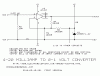
OK, here's my suggested circuit.

attachment.php

This shows a single stage. The 1.2V reference is included, and its output voltage can be fed to other stages like this one.

I have specified an OP-07 op-amp which has a much tighter input offset voltage specification than the MCP604x. This is important for accuracy at the relatively low voltages that the circuit deals with. You can use a trimpot to adjust the offset voltage; see the data sheet.

It needs to be powered from a split supply. I suggest +/- 5V. Decoupling capacitors should be used from pin 7 to 0V and from pin 4 to 0V on each op-amp. Filtering capacitors may be appropriate to improve noise rejection but there's little point bypassing the feedback resistor with a capacitor because the stage gain is pretty low.

The circuit uses four resistors with critical values.

Rs is the input shunt resistor that converts the input current into a voltage on the non-inverting input. I have shown a 10 ohm resistor on the schematic, but values up to around 40 ohms can be used, and higher values will make the circuit less affected by the op-amp's input offset voltage.

Rf (feedback), Rg (ground) and Rb (bias) connect at a summing node at the inverting input of the op-amp. The ratios between their values are interrelated, and must be correct to give the correct gain and DC offset. Rf can be calculated fairly easily once Rb and Rg have been chosen, but I haven't figured out how to calculate the ratio of Rb to Rg. It may be beyond my maths ability to give you a formula for that ratio.

Here are some explanations and calculations.

The difference in voltage at the op-amp's non-inverting ("+") input, over the 4~20 mA input current range, I will call dIN. It's defined as Rs * 0.016.

The gain of the amplifier I will call G. For an output range of 0~1V, G needs to be 1 / dIN.

G is determined by the ratio of Rf to (Rb || Rg). (The expression Rb || Rg means Rb in parallel with Rg, and can be calculated as 1 / ((1/Rb) + (1/Rg)).)

Specifically, you can calculate the correct value for Rf by calculating (Rb || Rg) and multiplying it by G-1.

As for calculating the ratio of Rb to Rg, I'm not sure how to do that. My maths skills are probably not up to working it out either. I used trial and error and the attached spreadsheet.

Here are a few Rb values for different values of Rs (the input shunt resistance). These all assume Rg is 1000 ohms:

Rs = 10 ohms; Rb = 24200 ohms.
Rs = 20 ohms; Rb = 9200 ohms.
Rs = 22 ohms; Rb = 7836.36363636 ohms.
Rs = 33 ohms; Rb = 3290.9090909091 ohms.
Rs = 47 ohms; Rb = 582.9787234043 ohms.
Rs = 50 ohms; Rb = 200 ohms.

In all of these cases, Rf needs to be changed as well; the attached spreadsheet calculates the value for Rf according to the formula above.
 

Attachments

  • T267475.001.GIF
    T267475.001.GIF
    5.8 KB · Views: 208
  • t267475.zip
    2.1 KB · Views: 69
Last edited:

KrisBlueNZ

Sadly passed away in 2015
Nov 28, 2011
8,393
Joined
Nov 28, 2011
Messages
8,393
The 1.2V reference voltage at the reference IC is regulated by the reference IC and does not change significantly depending on the amount of current that is being drawn from the reference (within reasonable limits).

Once you feed that voltage through a voltage divider made from resistors, the output from the voltage divider is no longer regulated against changes caused by changes in the current drawn from that point.

So in your circuit, current flows from the op-amp's output, through R3, through R4, and into the voltage divider. The direction and amount of this current depends on whether the op-amp's output voltage is higher or lower than the voltage divider's output voltage, and by how much.

This current causes the voltage at the voltage divider output to change, because the voltage divider output has a non-zero output impedance.

You can calculate the output impedance of a two-resistor voltage divider with fixed voltages on the ends of the resistors by calculating the parallel resistance of the two resistors.

In this circuit, the resistors are 3k8 and 1k0. Those values in parallel work out to about 792 ohms. You can reduce R4 by 792 ohms to take this into account, but you won't be able to use that 250 mV reference voltage for the other circuits in your project, because it's not stable.
 

sid2286

Aug 24, 2011
102
Joined
Aug 24, 2011
Messages
102
Thank you for your reply,

I tried using 9.2R resistor in feedback (in place of R4) but that is not helping., I am not using the reference i.e 1.2V for anything else.
Moreover the what i observed was that the resistance of (R7 and R9) is changing when R6 is connected,.,.

So i removed the zener and shot linked R6 to get a reference directly from 5V using a combination of 19K at R7 and 1K at R8 to generate 250mV, which I get but that too is changing when I change the current from 4mA to 20mA.

I want to use the same circuit since I already got the PCB designed,

what should I do next., I need to keep 250mV constant (which I know) but dont know how ?

Please suggest.
Sid
 
Top