Maker Pro
Maker Pro

Transistors

BobK

Jan 5, 2010
7,682
Joined
Jan 5, 2010
Messages
7,682
Show me your design procedure then that does not refer to controlling the Ib. Once you have done that, you have embraced the voltage control model.

Bob
Your last sentence would apply to 100% in case I could know the exact Vbe value which belongs to the desired current.. However, as we all know this is not the case and, therefore, we apply negative feedback in practice. It is easy to show that in this case, it practically does not matter if I use 0.65 volts or 0.7 volts for calculation.
My bolding.

Yes, and that is exactly why the designer treats the BJT as a device controlled by current rather than voltage.

Bob
 

(*steve*)

¡sǝpodᴉʇuɐ ǝɥʇ ɹɐǝɥd
Moderator
Jan 21, 2010
25,510
Joined
Jan 21, 2010
Messages
25,510
This is a model used to explain a transistor via the current control method:
Current control.png
I assert this as a method of current control because we have no ides what the base voltage is. We can estimate the base current, and indeed the high value of resistance chosen swamps out all but the estimate of a constant VBE.

And this is one that you would use to describe voltage control:

Voltage control.png
We all know that the second one relates more to the actual physics of the transistor.

However I will strongly assert that we very rarely concern ourselves with the actual very small changes in VBE which actually control the transistor. Yes, it is undeniable that the BJT is controlled by the electric field generated by the difference in potential between the base and the emitter terminal, and that it does so even when that electric field exists in the absence of the ability for current to flow.

However, in almost all practical applications we take advantage of the fact that when we are between cutoff and saturation there is a relationship between IC and IB that is substantially linear over some range of IC around an operating point which in turn allows us to threat the transistor as a fairly simple device.

In the words of some introductory texts, the resistor R1 in the first example "converts the voltage into a current".
 

LvW

Apr 12, 2014
604
Joined
Apr 12, 2014
Messages
604
Yes, and that is exactly why the designer treats the BJT as a device controlled by current rather than voltage.
Bob

Bob - may I ask you: At which design step?
Again, I like to refer to my post#65 which lists a typical design procedure for a common emitter amplifier.
I cannot see any step in which the designer "treats the BJT" as current-controlled device. Am I wrong?

And this is excactly the point which surprises me and which I do not understand:
People who consider the BJT as current controlled argue that this would be the most simple working model for designing BJT amplifiers.
However, as far as I can see (and I wait for counter examples), there is no single design step that makes use of current-control model.
Instead, they use the VOLTAGE Vbe during calculation of the operating point.
This is, of course, also true for a design with a base resistor Rb only (instead of a voltage divider).
I know that it is common practice to say that we "inject a current" into the base. However, to be exact: This is not the case.
During calculation of Rb we again have to use the value of 0.65..0.7 Volts as an input and - in fact - we have a voltage division between Rb and the resistance of the B-E path,
which allows the voltage drop we have used for this calculation. Such a current is always the result of a driving voltage.
And this applies also to the 1st circuit as shown in Steve´s recent contribution.
An external circuitry can never influence the internal working principle of the BJT.

In summary: There is a base current that cannot be avoided and which, of course, is to be taken into account during the design process (resistor calculation).
However, there is no design step which really makes use of the claim that the BJT would be treated as current-controlled.
Therefore: Why the whole discussion?
 
Last edited:

(*steve*)

¡sǝpodᴉʇuɐ ǝɥʇ ɹɐǝɥd
Moderator
Jan 21, 2010
25,510
Joined
Jan 21, 2010
Messages
25,510
However, there is no design step which really makes use of the claim that the BJT would be treated as current-controlled.
Therefore: Why the whole discussion?

In the following circuit, what voltage should I use to bias the transistor reliably into saturation without damage to the transistor?

voltage-control-png.12455

Now replace V1 with a current source and tell me what current should I use to bias the transistor reliably into saturation without damage to the transistor?
 

BobK

Jan 5, 2010
7,682
Joined
Jan 5, 2010
Messages
7,682
Bob - may I ask you: At which design step?
For the second time, this one:

* Calculate two resistors for proper base DC biasing - based on a suitable voltage Vbe (0.65...0.7V).
For this calculation, of course, the DC base current Ib=Ic/beta is used (because it exists and its existence was never denied).

You are using a roughly estimated Vbe, then calculating the bias based on the current Ib. This is what Steve are I are calling a current control model. As Steve has also said, this step, if using a voltage control model, should be to calculate the exact Vbe needed, then determine the biasing resistors to achieve that Vbe. Which you cannot do because a small change in Vbe will wildly vary the current and will not be consistent from device to device.

Bob
 

Arouse1973

Adam
Dec 18, 2013
5,178
Joined
Dec 18, 2013
Messages
5,178
I always use this for my design process. I thought everybody did?. Everyone knows 0.7V with and idility value of 1 = 2000Amps with no base resistor don't they.;)
 

Attachments

  • upload_2014-4-17_13-57-21.png
    upload_2014-4-17_13-57-21.png
    23.8 KB · Views: 120

LvW

Apr 12, 2014
604
Joined
Apr 12, 2014
Messages
604
In the following circuit, what voltage should I use to bias the transistor reliably into saturation without damage to the transistor?

voltage-control-png.12455

Now replace V1 with a current source and tell me what current should I use to bias the transistor reliably into saturation without damage to the transistor?

Hi Steve, I am afraid, there is a deep misunderstanding between us. Nevertheless, at first, I will answer your question:
1.) As you know, the voltage V1 should be in the range 0.6...0.7 Volts. However, this biasing scheme makes absolutely no sense because the transfer function Ic=f(Vbe) has very large tolerances. More than that, there is no temperature stabilization and the stage cannot be used as an amplifier because of zero input resistance.

2.) I think, replacing V1 with a current source will not much improve the situation because the relation Ib=Ic/beta also is equipped with large tolerances - nevertheless, I confess that the danger of damage may be smaller in this case. This is not surprising because the series resistor Rb used to convert a voltage into a current acts as a protection resistor (similar to the series resistor in a simple Z-diode stabilization circuit). But remember: Rb is caculated using the difference between the external voltage and the assumed Vbe value. Hence, the calculated Rb value ensures that the selected current Ib causes such a voltage drop across Rb so that the remaining voltage (Vbe) is as initially assumed. This means (in short): At first we have the voltages and the current is the result.

3.) Now - regarding the mentioned misunderstanding: For my opinion, both of your examples cannot say anything about the main question we are discussing in this thread:
Which electrical quantity controls the collector current Ic (Vbe or Ib) ?
You have shown two extremely different methods for biasing the transistor - and everybody knows, that both alternatives cannot be used in practice.
But the misunderstanding - as far as I can see - is the following:
Your circuit No. 2 (current source instead of v1) looks as if we would inject a current into the base which then would control Ic. And indeed - doubling Ib will double Ic. And therefore you are using the term "current control model". And I agree: This works as a model!
However, my understanding of "control" is not based on a model but rather on physical phenomena (and this seems to be the only difference between our understandings).

4.) Earlier I have mentioned the thickness of the depletion layer which undoubtly is altered due to the changing VOLTAGE across the junction.
As another physical parameter I like to mention the temperature dependence of the collector current:
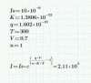
We all know the value of app. (dVbe/dT) = -2mV/K (for Ic=const). This is another clear indication that Ic depends on Vbe.
Question: Is there any equivalent figure (dIb/dT) which tells us how to reduce Ib for a 1K temperature increase to keep Ic constant?
 
Last edited:

LvW

Apr 12, 2014
604
Joined
Apr 12, 2014
Messages
604
You are using a roughly estimated Vbe, then calculating the bias based on the current Ib. This is what Steve are I are calling a current control model. As Steve has also said, this step, if using a voltage control model, should be to calculate the exact Vbe needed, then determine the biasing resistors to achieve that Vbe. Which you cannot do because a small change in Vbe will wildly vary the current and will not be consistent from device to device.
Bob

Hi Bob - please read my response to Steve´s post - I suppose, there is the same misunderstanding between us regarding the term "control".
Nevertheless, thank you for your answer.
 

(*steve*)

¡sǝpodᴉʇuɐ ǝɥʇ ɹɐǝɥd
Moderator
Jan 21, 2010
25,510
Joined
Jan 21, 2010
Messages
25,510
Hi Steve, I am afraid, there is a deep misunderstanding between us. Nevertheless, at first, I will answer your question:
1.) As you know, the voltage V1 should be in the range 0.6...0.7 Volts. However, this biasing scheme makes absolutely no sense because the transfer function Ic=f(Vbe) has very large tolerances. More than that, there is no temperature stabilization and the stage cannot be used as an amplifier because of zero input resistance.

So let me get this straight. You WOULD NOT advocate for using a directly applied voltage source (referenced to the emitter) to the base of a transistor to control it?

edit: the voltage source *IS* your signal.
 

Ratch

Mar 10, 2013
1,099
Joined
Mar 10, 2013
Messages
1,099
Everyone should read the link in post #69, where Winfield Hill illustrates the voltage control vs current control design philosophy. Very interesting read.

Ratch
 

(*steve*)

¡sǝpodᴉʇuɐ ǝɥʇ ɹɐǝɥd
Moderator
Jan 21, 2010
25,510
Joined
Jan 21, 2010
Messages
25,510
Everyone should read the link in post #69, where Winfield Hill illustrates the voltage control vs current control design philosophy. Very interesting read.

It certainly backs up everything I've said.

Totally true, but (for the beginner) practically useless, misleading, and dangerous.
 

LvW

Apr 12, 2014
604
Joined
Apr 12, 2014
Messages
604
So let me get this straight. You WOULD NOT advocate for using a directly applied voltage source (referenced to the emitter) to the base of a transistor to control it?
.
Of course not (between base and emitter). Or did you expect another answer (I am not a beginner) ? In each of my contributions I have mentioned the necessity of having dc negative feedback (as you know - because of tolerances and temperature stability).
 

(*steve*)

¡sǝpodᴉʇuɐ ǝɥʇ ɹɐǝɥd
Moderator
Jan 21, 2010
25,510
Joined
Jan 21, 2010
Messages
25,510
Of course not (between base and emitter). Or did you expect another answer (I am not a beginner) ? In each of my contributions I have mentioned the necessity of having dc negative feedback (as you know - because of tolerances and temperature stability).

And yet you advocate that voltage control is practically useful.

Negative feedback applies to the control of a system, not a transistor. In this case the system might be a common emitter amplifier with an emitter resistor. And even though you might call your method "voltage control of the transistor", nothing in your explanation describes the actual fundamental physics of VBE changing in order to facilitate the larger electric field which drags more charge carriers into the base.
 

LvW

Apr 12, 2014
604
Joined
Apr 12, 2014
Messages
604
I think, it´s time to find a summary. Let me try it (my view):
* As a stand-alone element and with an appropriate C-E voltage the transistor (BJT) can deliver a collector current that undoubtly is controlled by a voltage that exist across the B-E junction.
That means: The BJT can be seen as a voltage controlled current source (VCCS) - and, hence, its transfer characteristic is described using the transconductance gm (slope of the Ic=f(Vbe) curve). The transconductance gm is the key parameter that determines the gain capabilitiy of the device.
It is to be mentioned that this VCCS is a non-ideal device because the input voltage causes a corresponding input current Ib.

* For practical use the BJT is equipped with passive elements to allow operation as an amplifier (biasing, operational point, current-voltage conversion, stabilizing feedback).
For proper calculation of corresponding resistor values the whole circuit (BJT with external elements) can be treated as a current controlled amplifying block because we can exploit a simple
relationship between collector and base current Ic=beta*Ib.

Comments and corrections are welcome.
 

LvW

Apr 12, 2014
604
Joined
Apr 12, 2014
Messages
604
And even though you might call your method "voltage control of the transistor", nothing in your explanation describes the actual fundamental physics of VBE changing in order to facilitate the larger electric field which drags more charge carriers into the base.
Yes - you are right. I didn´t explain the "fundamental physics" of the BE junction (minorities, majorities, diffusion, recombination,...) I am not a specialist for this.
For my opinion (and for the purpose of this thread) , it was sufficient to see the relationsip to the pn junction of a diode - in particular the similarity of the effects a voltage has on the thickness of the depletion zone and, hence, on the current through it.
 

(*steve*)

¡sǝpodᴉʇuɐ ǝɥʇ ɹɐǝɥd
Moderator
Jan 21, 2010
25,510
Joined
Jan 21, 2010
Messages
25,510
Comments and corrections are welcome.

I think we are in agreement.

edit: and I think we were arguing slightly different things, so please forgive me for my somewhat less than tolerant replies to some of your posts.
 

Ratch

Mar 10, 2013
1,099
Joined
Mar 10, 2013
Messages
1,099
And yet you advocate that voltage control is practically useful.

Negative feedback applies to the control of a system, not a transistor. In this case the system might be a common emitter amplifier with an emitter resistor. And even though you might call your method "voltage control of the transistor", nothing in your explanation describes the actual fundamental physics of VBE changing in order to facilitate the larger electric field which drags more charge carriers into the base.

Well, there is not a "large electric field" that attracts/repells more charge carriers into the base. A BJT is a diffusion device. From the moment the PN junction of the BJT is manufactured, the holes from the P-type material will diffuse into the N-type material and vice versa. The electrons and holes will annihilate each other and create a depletion region between the PN junction where the concentration of movable charge carriers is very low due to annililation. This depletion region has a barrier voltage along its boundary caused by the immovable ions that were created when they relinquished their diffusion carriers. This voltage is of such polarity so as to oppose any further diffusion. Therefore, more diffusion causes more opposing barrier voltage, which in turn causes the diffusion to stop when an equilibrium is reached. This is the state the BJT will maintain from the factory to the circuit. In the circuit, a forward Vbe will be applied, the barrier voltage will be lowered, and the heavily doped emitter will will send its charge carriers into the very thin base region. Most of these charge carriers will be attracted by voltage of the forward biased collector. A small percentage of carriers will escape the attraction of the collector, and go into the base where they don't do any good, and can be considered "waste current". The entire purpose of the base-emitter diode is to bring the charge carriers into the base region by diffusion. Then they are swept into the collector not by diffusion, but by voltage attraction. No matter what the collector voltage, it cannot receive more charges than are available from the emitter supplied base. That is why the Ic-Vc curve is flat in the active region. In summary, the Vbe controls the collector current exponentially by diffusion regulation. The Ib is an unavoidable useless loss or waste current that does nothing to control the collector current. Ib is also exponentially related to Vbe, and thereby also related to Ic.

Winfield Hill talks about voltage-centric or current-centric design methods. Basically, current-centric design uses the relationship Ib has with Ic. It relies on Beta being sufficient to provide enough feedback to overcome variations in component parameters. Winfield prefers the voltage-centric method. He sets the quiesient current by applying a bias voltage and signal across the emitter resistance. Therefore Beta is not a factor and Vbe is automatically set to whatever it takes to maintain the collector current. The design choice is yours, but I highly recommend all to read the link provided earlier.

Ratch
 
  • Like
Reactions: LvW

LvW

Apr 12, 2014
604
Joined
Apr 12, 2014
Messages
604
I think we are in agreement.
edit: and I think we were arguing slightly different things, so please forgive me for my somewhat less than tolerant replies to some of your posts.

It´s OK - no problem.
LvW
 

Arouse1973

Adam
Dec 18, 2013
5,178
Joined
Dec 18, 2013
Messages
5,178
Hi Ratch
I must say what a very good explanation of how a BJT works . I am a bit confused well it don't take much. I was once told in a post that if I wanted to be pendantic then a BJT was in fact a field effect device. I was not sure but ended up using this in a presentation amongst other technical people at work. They looked at me. Bit confused I must say. But thinking I had been educated on here I felt quite confident.It appears they might have been wrong.

If this is the case then I am pissed to be honest.
Now this person might have been on about the electric field that is developed between the BE junction that pushes the electrons into the bases neutral region. I am not sure.
So I am now confused about the whole electric field thing.

I thought that if you had a potential difference you had an electric field between the two so more charge on one side than the other. And in a transistor say the collector is higher porential than the emmiter you have an elctric field between the two so why don,t you have one across the base emmiter juntion which pushes electrons into the base. Then does this not match what Steve is saying.

If not can you explain the difference.
I understand that the BJT is a diffusion device and it does not need an electric field to do so. But it does this because of the difference of charge between the emitter and collector. But if this charge difference is a potential difference why is there not an electric field.
Thanks
Adam
 
Top