Maker Pro
Maker Pro

Understanding a 5-transistor radio circuit

snake0

Mar 30, 2014
54
Joined
Mar 30, 2014
Messages
54
Hi there, I have been leafing through the excellent transistor circuit samples over at talkingelectronics.com, however they provide quite a minimal degree of commentary on each circuit, and while I feel I am gaining an understanding I wish to make sure I have understood it right.

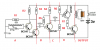
In particular I am looking at the 5 transistor radio as shown in the attached picture. I will state how I understand the circuit below, if anyone could point out errors in my understanding I would be very grateful.

Stage A: 10n between (+) and (-) stabilizes voltage
R1 100k resistor provides V splitter with R3 100k/110k * 3V = 2.7V, applied to antenna coil
Output of antenna is fed to a darlington pair of BC547s,which amplify the antenna signal twice. Output is sent across 100n staging capacitor to stage B in the form of varying voltage.

Stage B: signal from Stage A is sent into another transistor to be amplified.
Voltage splitter of 10k+220k ensure that the 100n staging cap going into stage C receives 220k/230k * 3V = 2.86V at peak. Stage A signal turns base of stage B trans on/off, which turns current through transistor on/off, which turns voltage at the 100n staging cap going into stage C on/off. (Why is this stage necessary? more amplification of signal?)

Stage C: Output from stage B is sent into base of PNP transistor, which is connected to another NPN below (darlington pair). R6 and R8 divide voltage giving 47k/57k *3V = 2.47V at base of PNP trans (if there is so much voltage here already how does the stage C staging cap influence the base? also why is so much voltage required for just the base of a transistor?)
Varying current through the NPN below the PNP flows through a transformer and speaker (the transformer brings the voltage down to half? why?) - which outputs the sound.


As you can see from my questions in parentheses, I am not quite sure of the purpose of some of these components. Any advice would be appreciated!
 

Attachments

  • 5transradio.png
    5transradio.png
    33.4 KB · Views: 516

Arouse1973

Adam
Dec 18, 2013
5,178
Joined
Dec 18, 2013
Messages
5,178
The 10n is probably a filter for noise and to stabilise the operating point of the transistor. The 100K biases the transistors the first transistor is only just on but the second one is fully on with only 1V on it collector. It is held out of saturation by the feed back resistor and this provides negative feedback to help with thermal runaway and increases switching speed versus a saturated transistor biasing. The Darlington arrangement normally has the collectors tied together, so I would say this was just a high gain transistor stage.The other stage is just another amplifier with biasing resistors to just start to turn on the transistor and the signal is coupled in to this stage via the capacitor. The output is then fed to the speaker driver, again this is not a Darlington.
Adam
 

(*steve*)

¡sǝpodᴉʇuɐ ǝɥʇ ɹɐǝɥd
Moderator
Jan 21, 2010
25,510
Joined
Jan 21, 2010
Messages
25,510
The 10n cap provides a low impedance at the radio frequency, and a very high one at DC. This allows the signal to be ground referenced without disturbing the DC bias of the first stage.

It is more common to see the cap connected between the biasing and the input rather than placing the input between the biasing and the base. In this case it's essentially equivalent.
 

snake0

Mar 30, 2014
54
Joined
Mar 30, 2014
Messages
54
I redid the pic as the stages were wrong

I can see now that stage B is the common emitter configuration which amplifies VOLTAGE i.e. the signal from stage A

However stage C also seems to use this, although I would have thought that the speaker requires increased current so it is strange that stage C isnt common collector configuration. I guess the transformer does that instead.

It turns out the two transistors in stage A are a replacement for the 'radio in a chip' ZN414 which produce a tuned radio frequency, but how this is being done here in the transistor version without any capacitors is another puzzle..
 

Attachments

  • 5transradio.png
    5transradio.png
    38.2 KB · Views: 218
  • 5transradio.png
    5transradio.png
    38.2 KB · Views: 144
Last edited:

Arouse1973

Adam
Dec 18, 2013
5,178
Joined
Dec 18, 2013
Messages
5,178
The 10n cap provides a low impedance at the radio frequency, and a very high one at DC. This allows the signal to be ground referenced without disturbing the DC bias of the first stage.

It is more common to see the cap connected between the biasing and the input rather than placing the input between the biasing and the base. In this case it's essentially equivalent.

Good point Steve about 10n, missed that point.
Adam
 

Arouse1973

Adam
Dec 18, 2013
5,178
Joined
Dec 18, 2013
Messages
5,178
Common collector is this configuration will supply approx. 260mA into 8R resistive load and the transistor will dissipate 240mW. In the configuration shown common emitter, the transistor will supply 340mA into a 8R resistive load and the transistor will dissipate 106mW. Can you see now why this method was chosen? Don't drive heavy loads in this way if you can kelp it because it wastes power.
Adam
 

duke37

Jan 9, 2011
5,364
Joined
Jan 9, 2011
Messages
5,364
The first two transistors do not do the same thing as a ZN414, they are merlely a high input impedance amplifier.
The ZN414 has a high input impedance but has automatic gain control and a detector. The ZN414 is obsolete but there is a modern equivalent.
 

snake0

Mar 30, 2014
54
Joined
Mar 30, 2014
Messages
54
Ok I have delved into the allaboutcircuits book on semiconductors, which has a great discussion about biasing techniques, now I have come back to reanalyze this radio, actually I'm just looking at the amplifier part which is taken from an easier circuit called the 'super ear'.

I thought I understood it but my calculations aren't coming up with the right answers. See below:


upload_2014-4-19_15-38-40.png

Q1
type: common emitter
collector feedback bias
class A

--Emitter current--
Vcc = 3v
Rc = 10k
Rb = 220k
Beta = 100
Ie = (3v-0.7v)/((220k/100)+10k)=188uA

--Collector voltage--
Vc = Vcc - IcRc
= 3v - (0.189mA*10k) = 1.11v

Q2
type: common emitter
voltage divider bias
class A

--Emitter current--
Vcc=3V
Rb=Rth
R1 = 10k
R2 = 47
Rth = 1/(1/R1+1/R2)=8.246k
Vth = Vcc * Rth/R1 = 2.47V
Vbb = Vth
Rb = Rth
Re = 0
Beta = 100
Ie = (Vbb - Vbe) / (Rb/B + Re)
= (2.47V - 0.7V) / (8.2k/100) = 21.6mA

Vc = ???? (I don't know how to work this out as collector is tied to Q3)

The brief description in the book says this:
"The second and third transistors are not turned on during idle conditions and the quiescent current is just 5mA.
The biasing of the middle transistor is set for 3v supply"

Well, I didn't get 5mA but that is probably my calculation error, but with regards to the middle transistor (Q2) this doesn't make sense to me. If it is supposed to be biased for 3V then surely the Vc should be midrail (1.5V). Now I am fairly sure my calculation for the bias voltage of 2.47 is correct since its just a simple voltage divider. Why is it 2.47V?

Also I tried building this in the simulator but it goes all screwy at the output to Q2:

upload_2014-4-19_15-49-52.png
As you can see, Q2's output (yellow) is being enormously clipped and is obviously wrong.
 

Attachments

  • upload_2014-4-19_15-48-33.png
    upload_2014-4-19_15-48-33.png
    308.3 KB · Views: 138
  • upload_2014-4-19_15-49-28.png
    upload_2014-4-19_15-49-28.png
    85.8 KB · Views: 115

snake0

Mar 30, 2014
54
Joined
Mar 30, 2014
Messages
54
Analysis of stage 1:

upload_2014-4-19_16-20-47.png

Stage 1 gains:
voltage = 2.24V/0.07V = 32
current = 156uA/19.6uA = 8

Ie is lower than my estimate of .189mA probably due to a gain lower than 100, however..

Vc = Vcc - Ic*Rc = 3V - (0.156mA * 10kohm) = 1.44V
calculation is way off, voltage in simulator is 1.91V
 

snake0

Mar 30, 2014
54
Joined
Mar 30, 2014
Messages
54
Analysis of Stage 2:

Ok so the base of Q2 is ~3.1V when the signal is added - perhaps that is what the book meant by 'biased to be at 3V'.
Gains:
1.4V/3.15V = 0.44
1.4mA/.2mA = 7
So a gain of 7 in current but the voltage is chopped in half.
As shown below, voltage has now lost its bottom half. Obviously something is wrong.

upload_2014-4-19_16-44-58.png
 

Attachments

  • upload_2014-4-19_16-44-19.png
    upload_2014-4-19_16-44-19.png
    50.8 KB · Views: 185

duke37

Jan 9, 2011
5,364
Joined
Jan 9, 2011
Messages
5,364
I do not have the time to go through your calculations.
However you say that Q2 is class A. This is not so. If you work from the emitter, The voltage divider will give about 0.5V, this is not enough to turn the transistor on. Thus Q2 is running in class B and is acting as a radio frequency detector. There is a resistor between Q2 and Q3 which limits the base current of Q3 to protect it in the presence of very strong signals.With low level input, you will get nothing out. With high level input you will get distortion due to the clipping. I wonder how much happy medium there is.
 

snake0

Mar 30, 2014
54
Joined
Mar 30, 2014
Messages
54
Ah, you are right, Q2 is normally switched off (PNP pulled high) so it is class B.

I will continue to update with my findings, it seems that every book gives a conflicting view on how the various numbers affect each other.
 
Top