.
Sir KSB . . . . .
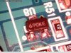
I also am having definition percepton limitations on the PCB's surrounding foil paths.
BUT . . . . most common normal component I.D. assignments are using R prefixes for resistors, C for capacitors, Q for transistors, and U for integrated circuits.
In this case of the U assignmant, the strongest initial consideration would be for a mere 3 terminal unit, to be a "3 terminal regulator".
Look closely at its interconnects and it seems that the power buss foil comes in at the right top of the device and connects to its central top connector and then
moves to the left and drops down and then loops over to the right of the device, thereby making a shorted connection.
Nope . . . . three terminal regulators don't utilize that "silly" manner of connections.
Considering that the unit might really be a transistor, if the top terminal is being its collector and looping down to short to the base ( left terminal) of the device, that would let a transistor
be used as a diode. (Producing the same junctions thermal tracking considerations that might compliment a like transistor used with it in adjunct circuitry)
The far right connection would be its emitter.
The nearby 4.7 k chip resistor seems to be shunting across the then created diode . . . . from power buss to emitter.
Aditionally, I wouldnt percieve of the unit as being a Zener diode , due to that shunting resistor.
What say you . . . .or others ?
73's de Edd
.


")

