edit: read Kris' post. Do what he says. But also measure the resistance of R8 and R9.
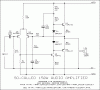
Q1 B to C = -17v; C to E= -0.5v; B to E =16v
Q2 B to E= -1.2v; B to C= 0.14v; C to E= 0.13v
These are a problem (or you have measured incorrectly.
The voltage between the collector of Q1 and the collector of Q2 should be 90 volts.
Please report the voltage from 0V to +45V and from 0V to -45V.
<-- Check this second
You show 0.63V. This means that the 0.33 ohm resistors (R8 and R9) have about 89.5 volts across them, thus a current of about 140A flowing through them (which I think is quite unlikely).
Are you sure R8 and R9 are 0.33 ohm resistors and not 33k resistors (or something similar)?
<--- check this first
The Q1's V
BE of 16 volts either means the device is in breakdown or you have measured poorly.
It would be useful to read these voltages with no speaker connected (assuming it was connected when these readings were taken), and to measure the voltage across the output and 0V (where the speaker would go). However this can probably wait.
Q4 B to E =3.8v; B to C=5.3v; C to E= -1.6v
The base to collector voltage again suggests that something is wrong with the output stage. I would be expecting around 45V here. These transistors have to withstand 45V (at the best of times), and up to 90V (in fault or clipping conditions) across the Base/Collector junction. The transistors listed there won't like that.
The V
BE suggests that Q4 is in cutoff (not a typical place for it to be in a long tailed pair like this). That would suggest the output is pulled fairly hard to one supply rail. This is not indicated by your voltage measurements for the output transistors, unless (as mentioned before) the resistors R8 and R9 are wrong, your power supply is very low, or (possibly) you have the speaker connected. And it would almost certainly require 2 out of three of those.
Once you verify a correct DC operating point (0V across the speaker with no signal, approx ) you can measure the voltage across one of these resistors to determine the current (again, no speaker connected). It should be between 0.0007V and 0.016V. I suspect you won't have a meter capable of measuring this.
Measuring the voltage across R8 and R9 will give you an idea of the quiescent current through the output transistors. Typically this is a small value (between a couple and maybe 50 mA). This design provides no way to adjust it and appears to result in one of the transistors being biased off.