Maker Pro
Maker Pro

SMPS boost regulator using a schmitt trigger oscillator

(*steve*)

¡sǝpodᴉʇuɐ ǝɥʇ ɹɐǝɥd
Moderator
Jan 21, 2010
25,510
Joined
Jan 21, 2010
Messages
25,510
Yesterday I was designing the board etc., for a 10V voltage reference I'm building.

For various reasons I want it to be battery powered, and because I need between 14 and 18 V input, I decided initially to use a pair of 9V batteries. This has the advantage of working until the batteries are *very* flat.

However, the box I'm building it in is about the size (internally) to fit 3 of these batteries, so (since the PCB will be the top of the box) I'm very limited in area. Most of it is actually taken up by the power switch and the nice gold plated banana sockets (bought because they're pretty, not for any really good reason).

OK, so it's getting squeezy.

I investigated what boost SMPS chips I have on hand, and I have nothing suitable.

A bit of googling shows up this site.

So I got to thinking... Can I make a simple oscillator using a Schmitt trigger inverter (you can get 2 of these in a SOT-23-6 chip) and drive a mosfet from them?

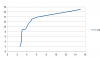
The answer is yes. And I managed to get 90V across the output (my load was 4k7). This was probably limited by the avalanche breakdown of the mosfet (60V) or the breakdown of the capacitor (63V).

To make this work, I creates a 50kHz oscillator using one schmitt trigger, and buffered it with another. The output is almost exactly 50% duty cycle.

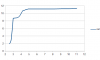
The mosfet is rated at just over 100mA, and the inductor was either a 5 ohm 2mH choke, or a 750uH inductor (of lower resistance and higher current capacity). The results from both were almost identical.

The next trick was to regulate this. What I did was place a series resistor between the oscillator and the buffer, and then tie the output voltage via a 10V zener and a 220 ohm resistor to the input of the buffer.

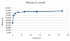
At an input voltage of around 8V at 6.3mA (yeah, flat battery), I achieved a stable 14.5V at (calculated) 3.1 mA, so an efficiency of 89% -- which I think is pretty good.

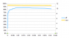
Note that the output voltage is not well regulated, it is based on the input voltage from the battery since the schmitt trigger's switching points are also dependant on supply voltage.

I have to go out now. If anyone is interested I can post a schematic later.
 

Electrobrains

Jan 2, 2012
259
Joined
Jan 2, 2012
Messages
259
I like that approach!
Small, cheap, efficient and unconventional (especially the way of regulating).
Yes, post the circuit diagram!
 

KrisBlueNZ

Sadly passed away in 2015
Nov 28, 2011
8,393
Joined
Nov 28, 2011
Messages
8,393
That's interesting Steve. I would be interested to see the schematic too.
 

(*steve*)

¡sǝpodᴉʇuɐ ǝɥʇ ɹɐǝɥd
Moderator
Jan 21, 2010
25,510
Joined
Jan 21, 2010
Messages
25,510
attachment.php


R1 10k
R2 47k
R3 4k7R
C1 4.7nF
C2 10uF 50V
D1 1N4150 (50V 250mA fast diode) -- A schottky diode would be better.
D2 1N4741 (11V Zener) (In series with another 1N4150)
D3 1N4150 (non-critical)
IC1 CD40106 Hex Schmitt trigger
Q1 2N7000
L1 2mH

Vout = Vz + Vin/2. Note that the zener is operating at a very low current ant the actual zener voltage may be significantly less than the specified value. In my case the 11V zener gave me a Vz of around 10V. With an input of about 8V, I got an output of 14.5V

"Regulated" here means that the output is controlled by feedback, it doesn't mean that it's particularly stable. It exhibits a marked sensitivity to line variations.

Without the Zener, the output voltage rises to the point at which something breaks. In my case I get around 90V, and it may be Q1, C2, or D1 that limits this.

The components shown here are probably good for up to 40V. It is a trivial matter to select more rugged components.

Some caution should be taken in the selection of Q1 as something with a very low Rds(on) is likely to have a high gate capacitance which will cause slow switching.

L1 can be anything that isn't going to saturate. This circuit is designed for low current, so a low inductance would not be recommended.

D1 needs to be a fast diode. The one I have here switches in 4ns. It happens to be one I have available in through hole, I'll probably use something else when I put this on a PCB.

D2 now has another diode in series with it (cathode to input of IC1b) so that if Vout is shorted, the mosfet won't be switched hard on.

My initial thoughts for IC1 were something like this, but they're only available in low voltage parts, and it turns out I actually don't have any on hand. So I'll probably use the 40106 (sop-14).

I'm considering if I will bother regulating the voltage to the 40106 to improve performance, but I expect that it won't be a huge issue.

I'm also considering knocking up another circuit like this with a variable constant current source so I can check breakdown characteristics of diodes, mosfets, etc.
 

Attachments

  • Scan-120819-0001.jpg
    Scan-120819-0001.jpg
    24.2 KB · Views: 642
  • Scan-120819-0001b.jpg
    Scan-120819-0001b.jpg
    24.9 KB · Views: 2,609
Last edited:

(*steve*)

¡sǝpodᴉʇuɐ ǝɥʇ ɹɐǝɥd
Moderator
Jan 21, 2010
25,510
Joined
Jan 21, 2010
Messages
25,510
For the inductor. First determine the mac current. For my circuit, the diode is 250mA, the mosfet 115mA, so let's say 100mA is the max current.

Since v = L di/dt, and v is (let's say) 9V, then 9/L = di/dt. Given a frequency f (therefore on time 1/(2f)) and maximum current i (100mA in this case) then

v/L >= 2.f.i

==> L >= v/(2.f.i)

from the figures calculated

L >= 9/(2 x 50000 x 0.1)
L >= 9/10000
L >= 900uH

And that's somewhat larger than I expected (especially considering my seat-of-the-pants choice of 750uH)

(Actually, considering that I had 8V, and possibly 0.5V across the mosfet, and up to 115mA through the mosfet, and my frequency was slightly higher than 50kHz, I could get away with something as small as 600uH, but it DOES indicate the perils of working by the seat of your pants!)
 

KrisBlueNZ

Sadly passed away in 2015
Nov 28, 2011
8,393
Joined
Nov 28, 2011
Messages
8,393
Cool Steve :)

I like circuits that look simple but have some level of ingenuity behind them. Your design has a low component count but still has closed loop voltage regulation.

As I understand it, your circuit uses on/off control of a fixed duty cycle signal; since U1A's output is a squarewave, you can't vary the duty cycle going to the MOSFET. Do you think it would be worth trying to implement duty cycle control by driving R2 from a triangle wave with a wide swing? I have a suggestion using two resistors and a capacitor to make the Schmitt oscillator input swing wider than the input thresholds so you could do this. Would reducing the "burstiness" of operation give any practical improvement in your application?
 

(*steve*)

¡sǝpodᴉʇuɐ ǝɥʇ ɹɐǝɥd
Moderator
Jan 21, 2010
25,510
Joined
Jan 21, 2010
Messages
25,510
Cool Steve :)

Thanks :)

As I understand it, your circuit uses on/off control of a fixed duty cycle signal; since U1A's output is a squarewave, you can't vary the duty cycle going to the MOSFET. Do you think it would be worth trying to implement duty cycle control by driving R2 from a triangle wave with a wide swing? I have a suggestion using two resistors and a capacitor to make the Schmitt oscillator input swing wider than the input thresholds so you could do this. Would reducing the "burstiness" of operation give any practical improvement in your application?

Funny you should mention that :D

My original idea was to use just a single schmitt trigger oscillator, driving the mosfet from that. The feed back was to be to the input of IC1a.

The rationale is that you have a triangular waveform here. Small amounts of additional current inserted here would (possibly) change the duty cycle, increasing the time the output stays low, and decreasing the time it stays high.

I had very poor results with this, having rather bizarre waveforms showing up at the gate of the mosfet.

It wasn't until after I reconfigured the circuit to be as you see here that I determined the cause was a very high impedance voltage source (otherwise known as an extremely flat battery).

It was something I was going to try again.

The advantage of the additional buffer is that the capacitance of the mosfet gate (and Miller effect) don't affect the oscillator.

At the moment, the circuit operates in discontinuous mode and it is impossible to see the bursts of activity on my scope (although I will admit to not actually trying very hard).
 

KrisBlueNZ

Sadly passed away in 2015
Nov 28, 2011
8,393
Joined
Nov 28, 2011
Messages
8,393
My original idea was to use just a single schmitt trigger oscillator, driving the mosfet from that. The feed back was to be to the input of IC1a. [...] It wasn't until after I reconfigured the circuit to be as you see here that I determined the cause was a very high impedance voltage source (otherwise known as an extremely flat battery).
That's an interesting idea. I'd be interested to know whether it works once you've installed a good battery. I kind of suspect it won't work very well. I think it's better to generate the control waveform independently of the voltage comparison.

I was going to upload what I thought was a nice answer to the problem, but I've just realised that it won't work. I thought that by generating a nice wide (approximate) triangle wave and feeding it into the buffer gate, and adding a DC offset derived from the zener, I could create a pulse width modulator. But no matter how you shift a (roughly) triangular wave up and down, the upper and lower thresholds of the Schmitt trigger will always be the same distance apart on the waveform. So that won't work at all!
At the moment, the circuit operates in discontinuous mode and it is impossible to see the bursts of activity on my scope (although I will admit to not actually trying very hard).
I guess it's probably not a problem then. I was thinking the constant start-stop behaviour might produce noise on the output, and/or audible noise from the inductor.

Have you considered sending it in to Electronic Design News "Design Ideas" or some similar column?
 

(*steve*)

¡sǝpodᴉʇuɐ ǝɥʇ ɹɐǝɥd
Moderator
Jan 21, 2010
25,510
Joined
Jan 21, 2010
Messages
25,510
Good news and bad news...

The good news is that it is possible to provide the feedback to the capacitor. It mucks up some of the waveforms though, so I'm not happy with it.

The bad news is that my original measurements of current omitted the current drawn by the oscillator (don't ask).

This was also beautifully masked by my use of a 47k load resistor rather than a 4.7k resistor.

Oh well.

The other thing is that the schematic is slightly wrong (text above has been updated) -- and it's even wronger!

The oscillator draws a fairly consistent 5mA, so the obvious thing to do is to try to reduce this. Well, I go and check the circuit because looking at the values I wrote down, the oscillator frequency simply can't be the values shown. It tuns out that the resistor is *much lower* in value. This explains almost 100% of the current (actually it seems to explain more than 100%, but that's probably the hysteresis of the 40106.

Anyway. The obvious thing is to change the capacitor and resistor to values that will reduce the current drawn by the oscillator.

So while, at the moment the actual efficiency is nothing like 89%, it (or something very close) is probably achievable. But that will be for tomorrow night...
 

(*steve*)

¡sǝpodᴉʇuɐ ǝɥʇ ɹɐǝɥd
Moderator
Jan 21, 2010
25,510
Joined
Jan 21, 2010
Messages
25,510
All good news now!

attachment.php


I had a couple of problems. One of which was that I had managed to connect my Schmitt trigger oscillator with the inverter pointing the wrong way. With the new components, the frequency of oscillation is around 33kHz.

The current draw for the oscillator has now fallen from 6mA to a couple of uA.

As you can see from the graph above, the efficiency is pretty good from about 1.5mA right the way up to 54mA, which was as far as I dared go. The fact that the efficiency was still increasing at this point is encouraging.

At 55mA output, losses amount to around 110mW.

Since a reasonable guess at the dissipation of the rectifier diode is around 30mW, and the inductor, around 50mW, the actual dissipation of the mosfet is almost certainly around 30mW, which is actually really small. What is interesting is that the peak current through the mosfet must be around 200mA, and the specs tell me that the TO92 device is actually well within it's operating limit, and that even the surface mount version should be OK (so maybe I could have pushed the current higher...)

The specs also tell me I should be expecting a Rds of around 1.5 Ohms, which equates to a power dissipation of around 30mW, which seems to match what we have above.
 

Attachments

  • Eff.png
    Eff.png
    11 KB · Views: 1,422

KrisBlueNZ

Sadly passed away in 2015
Nov 28, 2011
8,393
Joined
Nov 28, 2011
Messages
8,393
That's brilliant Steve!

Could you post an updated list of component values?

Has the schematic changed at all?

What value and type of inductor are you using?

Are you still using the same rectifier?

Now that you've fixed the errors, have you tried applying the feedback at the capacitor again?

This is a nice little circuit. Seriously, I think you should submit it to a "design ideas" column. EDN pay USD 150 I think. That should make it worth the trouble!
 

(*steve*)

¡sǝpodᴉʇuɐ ǝɥʇ ɹɐǝɥd
Moderator
Jan 21, 2010
25,510
Joined
Jan 21, 2010
Messages
25,510
I have updated the component list. (And a new schematic will appear soon)

The major circuit changes are to values of components.

I have removed the gate resistor, and perhaps I'll try using the other gates in parallel to give better gate drive (maybe tomorrow night)

The other change is the addition of a diode.

I'm contemplating changing the feedback to give better line regulation. The load regulation is really good right now. The output varied less than 10mV from 0.3mA to 55 mA.

Yeah, I'll probably submit it to an Australian magazine.

edit: unfortunately the inductor is one that I don't have specs for (or indeed an accurate part number)
 
Last edited:

BlackMelon

Aug 7, 2012
188
Joined
Aug 7, 2012
Messages
188
Steve,Please re-explain your voltage regulation trick... and how the oscillator works..
I simulated your circuit, after the simulation has started,I put 12V to the inductor and observe the output, output voltage was shoot to 35V and then it was continually dropping until it reached 14V and was regulated at that value
Did it work correctly?
If I want to get more out put voltage to get 24V from 12V input.... what should I do?
Thank you
 

(*steve*)

¡sǝpodᴉʇuɐ ǝɥʇ ɹɐǝɥd
Moderator
Jan 21, 2010
25,510
Joined
Jan 21, 2010
Messages
25,510
It's all pretty standard, just with an unusual component choice.

The oscillator is a simple schmitt trigger oscillator. Look up the datasheet or one of the application notes covering schmitt triggers or CMOS oscillators and you'll find in described.

The second schmitt trigger is simply used to buffer the oscillator's output and to drive the mosfet.

Everything to the right of that is a totally standard configuration.

The feedback is essentially just the zener diode to pull the input of the driver high (and this the mosfet gate low), overriding the oscillator when the output reaches a certain voltage. The other diode simply prevents the oscillator from trying to drive the output directly, loading the circuit down and keeping the mosfet permanently on (which would let the smoke out).

Without a load, the output voltage could rise above the regulation limit, and at some point could force excess current through the input protection circuit for the driver. My next version will address this. With any luck, it might be tested this weekend.

To increase the output voltage, increase the zener voltage. Ensure that all the components affected (mosfet, rectifier, and capacitor) can handle the extra voltage. Note that in this version, the output voltage is quite dependant on the input voltage too. Wait for the next version :)
 
Last edited:

BlackMelon

Aug 7, 2012
188
Joined
Aug 7, 2012
Messages
188
Thank you steve....
I have some questions left from your reply
When the input voltage of schmitt trigger is more than 5V,I will get the 0V output if the trigger is active right?
because I am familiar with only pure digital circuit.... reverse 5V to 0V really makes sense for me but 20V to 0V I have never experienced
 

(*steve*)

¡sǝpodᴉʇuɐ ǝɥʇ ɹɐǝɥd
Moderator
Jan 21, 2010
25,510
Joined
Jan 21, 2010
Messages
25,510
Remember that my logic is running from approx 9V, not 5V.

The output goes low when the input rises above the logic 1 input threshold for the schmitt trigger. That is about 2/3 Vdd, or about 6V.

For that to occur (independent of the oscillator) the output voltage must rise above 6V + Vz + the forward drop for the other diode., so an 11V zener gives you an output near 18V. If the output rises above about 21V then the input will try to get pulled above Vdd and the input protection diodes will conduct. That's generally not a good idea unless the current is very small.
 

(*steve*)

¡sǝpodᴉʇuɐ ǝɥʇ ɹɐǝɥd
Moderator
Jan 21, 2010
25,510
Joined
Jan 21, 2010
Messages
25,510
Here's an update as promised.

Firstly a Vin vs Vout graph. I've said that this regulator exhibits a marked sensitivity to Vin, so I thought I should graph it. And there's some surprises!
attachment.php

Two surprising things.

Firstly that something really strange is going on between a Vin of about 3V and 6V. Clearly this circuit behaves poorly below 6V. This isn't too much of a concern as I designed it for operation from 9V.

It's not surprising that the output is dependant on Vin, but it is interesting (maybe surprising) that it is so linear.

Above 6V, it's almost exactly 0.35 x Vin + 11.8 V

But that's clearly not a great result, so I decided (as foreshadowed) to improve the feedback loop to remove it's interaction with the trigger levels of the Schmitt trigger.

OK, so the modification is to use the zener in a more traditional way to disable the oscillator.

attachment.php


Q2 is the first NPN small signal transistor I could lay my hands on. It was a BC546. R3 probably could be increased significantly in value, but I just used the value which was already in circuit.

This will actually alter the mark/space ratio of the oscillator, so the control is actually a little finessed than the earlier design. The fact that it now eliminates the major cause of sensitivity to Vin is pretty clear from the graph below:

attachment.php
Whilst the circuit has the same odd behaviour for low input voltages, at about 5V it is able to produce an output voltage which is maintained up to an input voltage of 11 volts. (After this point, the input can flow directly to the output, so the regulator ceases to regulate.)

I'll do another set of tests to show how efficiency changes with load, although I expect it to remain pretty much the same as before. I will probably alter the zener diode to achieve a higher output voltage to make the basis of the test as similar as possible.
 

Attachments

  • vinvsvout.png
    vinvsvout.png
    10.6 KB · Views: 1,156
  • vinvsvout2.png
    vinvsvout2.png
    9.7 KB · Views: 1,171
  • Circuit3.jpg
    Circuit3.jpg
    25.6 KB · Views: 1,568

(*steve*)

¡sǝpodᴉʇuɐ ǝɥʇ ɹɐǝɥd
Moderator
Jan 21, 2010
25,510
Joined
Jan 21, 2010
Messages
25,510
And here is the (possibly long awaited) graph of output voltage and efficiency with output current.

This was for an input voltage of just under 9V

attachment.php


At just over 50mA output current the efficiency fell to about 82% This isn't too bad since I was targetting an output current of less than 30mA.

I still haven't tweaked this to give a higher output voltage.

However I did increase R3 to 47K with apparently little effect on anything.
 

Attachments

  • Eff.png
    Eff.png
    13 KB · Views: 1,194

KrisBlueNZ

Sadly passed away in 2015
Nov 28, 2011
8,393
Joined
Nov 28, 2011
Messages
8,393
Cool Steve, thanks for the update.

I'd be interested to see its performance at a higher output voltage - maybe twice the input voltage. But it's just curiosity; don't feel obliged to do any testing you don't want to do!

I just noticed in post #17 in this thread, there's a resistor, R2, between the oscillator and the buffer which isn't needed (AFAIK).

BTW, this design is meant to vary the oscillator's duty cycle smoothly in response to the feedback, but have you looked at the oscillator with a scope to confirm that the variation is smooth and each cycle is the same? In other words, that there are no variations at a lower frequency, like every n cycles? I guess it wouldn't matter if there were; I'm just curious.

Do you think an even simpler design would be workable, using a single Schmitt gate, applying the feedback from the zener anode directly to the input of the oscillator? The MOSFET would be driven from the oscillator gate output. The higher the output voltage became, the more the gate input would be pulled upwards, and the shorter the high part of the output cycle would become.

That design wouldn't have very good regulation against supply voltage variations, but it would be pretty minimal - two resistors, the oscillator capacitor, the zener, a single-gate IC, the MOSFET, the inductor, the output diode and the output capacitor. Do you think it would work?
 

(*steve*)

¡sǝpodᴉʇuɐ ǝɥʇ ɹɐǝɥd
Moderator
Jan 21, 2010
25,510
Joined
Jan 21, 2010
Messages
25,510
Cool Steve, thanks for the update.

I'd be interested to see its performance at a higher output voltage - maybe twice the input voltage. But it's just curiosity; don't feel obliged to do any testing you don't want to do!

Yeah, I was planning to have an output voltage of around 14V to 15V, and since it's operating from a 9V battery, testing down to 7V Is probably reasonable.

I've just got to pull out another zener to set the voltage.

I also want to do some work on showing the output ripple and the oscillator waveform. I think both will be interesting.

I just noticed in post #17 in this thread, there's a resistor, R2, between the oscillator and the buffer which isn't needed (AFAIK).
Yep, no longer needed. It's still in there in case I go back to the original design.

Due to the high input impedance of the Schmitt trigger, it's not significant (but it is superfluous).

BTW, this design is meant to vary the oscillator's duty cycle smoothly in response to the feedback, but have you looked at the oscillator with a scope to confirm that the variation is smooth and each cycle is the same? In other words, that there are no variations at a lower frequency, like every n cycles? I guess it wouldn't matter if there were; I'm just curious.
Yeah, and I plan to look at that.

Do you think an even simpler design would be workable, using a single Schmitt gate, applying the feedback from the zener anode directly to the input of the oscillator? The MOSFET would be driven from the oscillator gate output. The higher the output voltage became, the more the gate input would be pulled upwards, and the shorter the high part of the output cycle would become.

That design wouldn't have very good regulation against supply voltage variations, but it would be pretty minimal - two resistors, the oscillator capacitor, the zener, a single-gate IC, the MOSFET, the inductor, the output diode and the output capacitor. Do you think it would work?
I'm pretty sure it would work. And it offers the possibility of using a single Schmitt trigger inverter which is available in a SOT-23-5 package. (Do these come with a 4000 series CMOS power supply voltage range though...? The answer is YES)

Since it's designed to operate from a 9V battery and provide power to a 10V regulator, the sensitivity to supply variation is not too significant.

Actually, another fortuitous combination is the Vgs(th) of the mosfet I'm using which protects the circuit from weird behaviour at very low input voltages (you can see that from some of the earlier graphs).
 
Top