Maker Pro
Maker Pro

Digital programmable CDI ignition for 2-stroke engines

bob weir

Sep 10, 2014
235
Joined
Sep 10, 2014
Messages
235
p 53 506 jpg Oct17 001.jpg
Oct 17
an error in earlier work this year has been found. last spring , april 18 & 29 were posted circuits showing
the 16F506 being used as a signal source for the 12F508. the idea is a good one. the error was with
the ADC part of that uC. by the scan posted here today can be read that there is no on-chip
voltage reference. this is the fact that i missed. that and how the ADC uses Vdd for a conversion reference , whatever it happens to be.
on p. 1 of the 506 data is found that the operating range is 2.0 to 5.5 V for Vdd.

in those 2 ckt's Vdd was made from 4 nimh batteries in series that slowly drained.
thus the ADRES register numbers were off high or low.
the circuit needs an external voltage regulator so that Vdd is 5.0 V. all the time.
the Vdd batteries for now will be 2 lithium ion cells in series for a nominal 8.4V to 6.0V range.
so even at the low end there is still more than enough voltage to overcome the dropout of the
78L05 to-92 pkg device that is being used. a new circuit sketch will show the 78L05 regulator
going to the 16F506 uC

in fact since there are several ADC pins on the 506 it would be good to use a 2'd one
to monitor the battery voltage and to sound an alarm buzzer when the incoming voltage to the
78L05 gets to 7V. by using 7V we have some breathing room to take action before
the battery voltage gets to a 6V danger level where permanent damage can occur.
 
Last edited:

bob weir

Sep 10, 2014
235
Joined
Sep 10, 2014
Messages
235
Oct 18
the post today has the purpose of showing a common error source.
made often by beginners to the baseline family of uC's.
while using the PICKIT-2 or PICKIT-3 uC programmer it is all too easy
to accidentally erase the chip contents. and along with the erased code
the factory installed OSCCAL value is lost too. its placed in the upper
most program memory address at the factory

i think the mid-range uC's and more advanced others now a days put
the OSCCAL value in a place more secure than program memory.

the result of not having the factory OSCCAL value is the internal '4 Mhz'
R-C clock is not running corrected. and the code that is measuring time
will return faulty values. off by +/- 10% in this example.

the following scope screen shots are based on a circuit , flow diagram
and assembly code posted last april 18.

the first 2 show the result of the code on p.2 lines 84 to 86. where
there is a delay between the TE of the -70 pulse and the LE of the-10 pulse.

the ADC & pot were used to get the number 100 , decimal, to multiply the
32uS subroutine by. looping 100 times should yield a delay of 3200 uS
with the cursor the measured times are 3240 uS for the good OSCCAL
and 3520 uS for the 506 uC w/o a good one.

you can find these numbers on the LCD image. in the upper left corner
are 7 lines of cursor data. the line we want is 'BX-AX:' .

you may find it a bit difficult to see the pulse edges , the pulses
having only a coded width of 3x32uS means the cursor itself
takes up a good part of the pulse width

the other 2 images are for the code on lines 94 to 96 , also on p.2 of the code.
here a delay of .010 sec is called for
in this case we measure 10.00 mS as expected. in the other we get 9.08 mS.

and if you missed the message during programming of a faulty OSCCAL for that
uC chip you could end up wasting time searching the code for the cause.

why the error is 10% long in one case and 10% short in the other for code
running in the same uC is a puzzle. i'd a thought they would be consistent
short or long but not both.

the step i take to deal with this OSCCAL placement is to record its value
the first time the uC is installed in the PICKIT programmer ZIF socket and read.
if lost or erased it can easily be re-installed with the PICKIT s/w
 

Attachments

  • 3240uS   70_10     yes , OSCCAL   Oct 18.jpg
    3240uS 70_10 yes , OSCCAL Oct 18.jpg
    69.2 KB · Views: 111
  • 3520uS  70_10    no OSCCAL           Oct 18.jpg
    3520uS 70_10 no OSCCAL Oct 18.jpg
    73 KB · Views: 104
  • 10.0 mS delay yes , OSCCAL.jpg
    78 KB · Views: 124
  • 9.08  mS delay     no OSCCAL.jpg
    9.08 mS delay no OSCCAL.jpg
    73 KB · Views: 92
Last edited:

bob weir

Sep 10, 2014
235
Joined
Sep 10, 2014
Messages
235
Oct 20
the post today is to alert you to some questionable test results . the scope is
the Rigol 4-channel DS1054 . and the 506 uC circuit is wired on a 400 point breadboard.
power is via 4 nimh batteries , about 5.2V and slowly dropping

summary : the code is suppose to spit out 3 pulses at particular spacing then stop.
the first spacing is due to the ADC and a pot providing a number. and the next spacing
is a fixed software delay.
depending on the Horiz time base chosen there will appear repeat sets of these 3 pulses.
the problem then is this : one does not know if the uC is acting up by looping when not
coded to do so. or if its the scope with the memory in the scope acting up by repeating
earlier data onto the LCD so that it makes it appear the uC is outputting a continuous
and repeating signal

the 8.jpg image is what was expected. and the spacing is good .
see that the time base is 500uS per division. good repeatability was gotten
in 'Single' mode and by cycling the +5V

the 9.jpg image shows unexpected repeats of the 3-set of pulses.
its time base is 2.00mS and it and 5.00 and 10.00 is where repeats happen too.
the repeat 3-sets are about .008 apart. a spacing not supported by code.
this could be a clue the scope is showing artifact.
..... on first viewing this scope screen image one is likely to assume
it means the uC is repeating the 3-pulses over and over.

the assembly code is posted here too for those of you who want to see it .
the code is meant to supply the 12F508 uC with the simulated flywheel -70 and -10
degree pulses plus a 2'd -70 pulse. recall that the CDI ignition code is written to
fire a pulse to the CDI board some delay after a -70 pulse. thus to do its job
it first needs a -70 and a-10 pulse to calculate the RPM and thus know where on
the timing curve the engine is then at. with that a 'known' then the delay-to-fire is
simple to determine. and this delay-to-fire is referenced to the next -70 pulse
occurrence. thus we need the 506 to provide a -70 , a -10 and then another -70.
with those 3 pulses the 508 has all the information from the engine it needs to fire a spark.

the tricky thing about the 508 code is its doing 2 things at once while the flywheel
is rotating from -70 on to -10 degrees. firstly at the -70 mark it resets TMR0 so it can
count in units of 32uS from a known starting point. and while it is counting in the
back ground we do a time delay in software to the point the fire pulse needs spit out.
fire pulses happen in the -30 to -10 deg range.

we get away with this , doing 2 things in parallel , by knowing the delay-to-fire
amount of time is always less than the time it takes to spin from -70 to-10 degrees.

if you know anything about the scope doing these repeat displays of
a 3-set of pulses that are coded to only happen once please write me.
[email protected]
 

Attachments

  • DS1Z_QuickPrint8.jpg
    DS1Z_QuickPrint8.jpg
    65.9 KB · Views: 101
  • DS1Z_QuickPrint9.jpg
    DS1Z_QuickPrint9.jpg
    68.4 KB · Views: 108
  • 16F506 test code Oct 20.txt
    3.6 KB · Views: 76
Last edited:

bob weir

Sep 10, 2014
235
Joined
Sep 10, 2014
Messages
235
Dec 7 ... the following is for those of you who want to skip buying Microchips 'Low Parts Count Demo board' and their Pickit-2 programmer. when one can throw the equivalent together from less costly ebay purchases.

...... with a plus being a traditional multi-hole solderless bread-board is a lot handier to use than the LPC demo bd.

the 170-hole bd. bd. shown is the one i use for programming only. then the uC is easily
moved to a 400-hole bd. bd. for circuit build and testing.

a safety reason to is in play here. by moving the uC from a board connected to the PC
we can eliminate a path to the AC lines for when we are working on the circuit under test.

the 18-zif is a socket already here for previous work with the Picaxe -18x uC.

note - this same wiring scheme as for the 508 works with a number of other uC's too.
as they happen to have identical top-end pin-function locations. when i find the list
of what all they are it will be posted.

note - the LPC board shows a 6'th pin not 5 like mine. see this at the top end above the
'690 20-pin uC in the LPC bd. 20-hole DIP socket. on the pickit-2 is a piece of masking tape. and this 6th pin is labeled 'TIG'. i dont know what it is for. needing to know it has not come up yet.

note - on the LPC bd. are four 2-hole and two 6-hole connectors soldered on by me.
the long 14-hole one on its upper right corner is stock


pk-2 altve dec 7 forum.jpg 011.JPG 010.JPG
 
Last edited:

bob weir

Sep 10, 2014
235
Joined
Sep 10, 2014
Messages
235
506_tst_1  dec 13.jpg Dec 13.
the oct 20 post had in it a problem with the scope showing non-existant signal repeats.
the cause of those repeats is still an unknown. a new idea has arisen since then.
via looking at the timeline of the signals and noting some large mS delays between pulses
with uS spacing . and then it all repeating.

the new idea is to just have the 506 uC emit 3 pulses then stop. and push
the reset switch to set up a repeat with ADRES the same or a new value. we avoid the scope
having to trap a whole bunch of signals we really dont need with their wildly varying spacing.

since we are using the reset pin on the 506 we have to set up the __CONFIG register
to read '_MCLRE_ON ' and then add a switch , 2 resistors and a 0.1 cap to deal with contact
bounce of the switch when its pushed.

the method of gathering these signals is changed too. instead of using the scope's 'auto' mode , 'single' is used instead. by 'single' just one sweep of the scope occurs. all you gotta do
is play with the H- time base until you get the signals spaced how you want them.
a bonus is catching the 'dummy' spacing between the first -70 pulse and the following fire pulse.

its a 'dummy' as it is a hard-coded value and not the result of the range-test section of code

the job the cdi uC , the 508 , has to do can be done with just 3 pulses. a -70 , a -10, and then
the next -70. its life is to just look at them over and over. and with information derived
from them know when to emit a fire-pulse to the cdi ckt bd.

the cdi uC , the 508, looks at the first 70 deg pulse and delays some time then emits a fire
pulse to the cdi ckt. bd. then it next looks for the 10 deg pulse. and records the time to it from
when the earlier 70 pulse arrived. next , after the 10 pulse arrives, it does some 'range-test'
work to get a fresh fire-delay value. then when the next 70 pulse comes along this new delay
value is applied and another fire pulse emitted. then these steps are all repeated .

this post is also bringing light to an error i have been making with my testing.
the practice has been to code both the 506 with its 70 and 10 pulse signals and apply them
to the 508 uC. the error was to not first test each uC for its stand-alone behavior.

for instance it was discovered the 508 was emitting a fire-pulse with no 70/10 input pulses.
and the 1054 was not showing the 10 pulse out of the 506, nor the 1'st 70 pulse either.
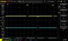
it turns out there is a icon at the top of the screen with a T in it for trigger. and it was
lining up with the first -70 pulse, and with the pulse having no side-lines its presence
was missed.

look above on the b/w LCD image and you can see this icon at the LE of the first
pulse on the CH 1 line. with a H=.002 sec spacing the top of this 96uS wide pulse
is narrow enough to be hidden by this icon.

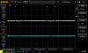
the material posted today is some 506 code that is well behaved. its output pulses
are shown on the scope screen image. the 70 and 10 pulses
emit with spacing = (ADRES) x (32uS) as coded. in this case ADRES is 10 hex for a
16x32 = 512 uS delay. and this is just the spacing seen on the 1054 screen image.

the ADRES is a result of the external pot and the amount of voltage on its output pin
that is read by the 506 AN2 input pin. you've seen this circuit before.

by the H=200us setting you can eyeball 512us between CH 1 TE to CH 2 LE.
and again 512 us from CH 2 TE to the 2'd CH 1 pulse's LE.

the careful reader will point out that the 2'd spacing , 10 to 70 is not the same as
70 to 10 on the engine. one is 60 deg or arc , and the other is about 300 deg.
ok , i fudged some. this was done to keep the signals all on the same scope screen image
with a small 200us H value. later , when the 506 and 508 are connected the delay from 10 to the next 70 will likely be increased. depending on how much 508 code has to run after
the -10 pulse is detected.


CH 1 is the simulated -70 deg pulse off the flywheel.
and CH 2 is the -10 deg pulse.

these 2 pulses represent all the information we get from the engine.
and it is enough for the 508 uC to determine when
to fire the spark according to the timing advance curve.

the code as a *.txt file was simply a faster way to post it. one sacrifices the line
numbers with this method. despite that though you can take it and re-label it
as a *.asm file and use the MPLAB Project Wizard and re-construct the project
from which it came. then print it out with line numbers if you so choose.
 

Attachments

  • 506_tst_1.txt
    3.2 KB · Views: 80
Last edited:

bob weir

Sep 10, 2014
235
Joined
Sep 10, 2014
Messages
235
dec 26
some other uC work has been getting in the way of this ignition coding effort.
many problems have come up. and a few are worth the mention. as they
could have some relevance for you too

the first was powering 2 bread-board circuits simultaneously. and seeing
the uC-ctrl'd led on the first board blink on then off then on. and the desired
audio output did not occur. it was learned that the 2'd board with its uC and other chips
and capacitors drew too much startup current.
this pulled down the +5 volt line to the point that the uC on the
first board reset. timing between these 2 uC's could not be met with this
happening and caused an output failure.

the solution was to undo just the wire to the 2'd board's uC. apply 5v to both
boards then touch the 5v wire to the 2'd board uC. in a second it sent out
the code with a serout command. and the 1'st uC had what it needed.
and its audio output then did happen.

the 1'st bd.bd. uC device being sent data is one of those little Catalex
mp3 board players with the 5300 chip sold on ebay for about $4


the lesson here was to attend to the turn-on times of uC's . and to add delay code
to the one uC that has data to send to the other uC. also learned that once the
uC with data to send has sent its data it can go into sleep mode as its job is done.

the next matter was my refurbished walmart desktop pc acting up.
it would run fine then at random reset itself. its behavior is not
acceptable and the 'blue screen of death' was the final straw.
it is pkg'd up for return. the 2-yr warr'ty will cover the refund.
and with their extended returns for the holidays the cost of
the warranty will be refunded as well


that w-m pc runs on w-7 and has a 9-pin -232 port on the back. it is
used to program the picaxe uC's that have been used on occasion
with this assembly coding ignition uC project.

so without a -232 port none of the picaxe uC's can be programmed.
this meant that it was finally time to install the Rev. Ed. AXE027 picaxe
usb cable and figure out how to update drivers for it.

Rev. Ed. has all one needs for this step at their website.
the 9 page introduction has the steps to follow to install the drivers.

the part that was new to understand was that the 027 cable
is itself a 'device' needing a driver. and so is the USB port it is plugged in to.
that port too needs a driver update.
... new too is that to use the 027 cable the same usb port needs to be used each time.

first my laptop was worked on and the s/w was loaded in about 20 min.
then came time to connect the cable end to a bread board with a -18x uC.
write a simple blink-a-led program and see if it would load. it didnt.
by switching the tx and rx wires it did load. and the uC ran at once too.
this sight brought on a feeling of joy.

next this was all repeated with my good HP desktop pc. and this time it went
easier. with the same end result. successful usb driver updates and picaxe
uC chip programming.

the bottom line is that for the first time ever both my Microchip uC's (12F508 et al)
and Picaxe uC's (08, 18x, 20M2 etc.) can be programmed with a USB cable.

so , now , a PC with a -232 port is no longer needed. and this type of pc can
join the other pc's : ( dos , w-95 , xp ), that served their time and are now obsolete
 

Attachments

  • serial -232.JPG
    serial -232.JPG
    306.2 KB · Views: 111
  • USB AXE027.JPG
    USB AXE027.JPG
    243.6 KB · Views: 110
Last edited:

bob weir

Sep 10, 2014
235
Joined
Sep 10, 2014
Messages
235
jan 18 .... update .
long ago , here on an earlier page , was posted ignition code work done by
a group SportDevices using a 16C84 uC.
their site is up & still includes the overview for this effort. including a circuit diagram and an assembly code file that can be downloaded. plus a mechanical disc that was used
to create test signals for the uC. here is the link.

http://www.sportdevices.co.uk/ignition/ignition.htm

at the time of finding their site my experience with assembly coding was too little to
want to try and tackle what they did. now things are different. and the confidence has
developed to at the least give it a look. and see how much can be figured out.
with the expectation of learning some of how they did it. and with hope of some take-aways
that can be used in my coding

with some head scratching their assembly code was turned into a project by the MPLAB
s/w 'Wizard'. and it did BUILD. and was next programmed onto a 16F84A with the
PicKit-2. for unknown reasons this programmer does not support a 16F84.
and no 16c84's are in my inventory to have tried them too.

yesterday a pulse 1-0-1 signal was applied to the '84A B0 pin to mimic what it gets from
the -72 deg coil at the flywheel. and the scope then monitored the A2 pin for a
'fire' pulse. i struck out. then later realized my RC clock was not verified to be 4M.
so today the RC is being replaced by a 4.0M xtal.

anyway as this all is peripheral to the other ongoing work on this posting i
thought it best to begin a new project posting. so as to not distract from the efforts
here with a baseline 12F508 uC. the 16C84 is a mid-range uC that has interrupt
ability. and the Sport Devices code does use it. for the purpose of detecting
when the TMR0 counter register overflows.

already the effort of trying to decipher someone else's code is paying off in
ways not anticipated. and it also puts me in the place of you , the readers of this
post, of what it is like to understand the code someone else wrote. when
even their best intentions to document what they are up to falls short
of presenting it in a manner fully in harmony with your style of learning.

the surprise is even with less notations than desired, nor any flow diagrams
to wish for there is still enough there for a stimulating time of thinking
about it all . and getting ideas of what to take a closer look at. and new ideas
of things to try. so one has lots of resources to summon up. starting with
your knowledge and then using your intelligence

one last thing to mention is another source of material for getting going
with assembly programming for these baseline and mid-range uC's.
ex. the first book by david benson called " Easy Pic'n " . and tho it
was written 20 years ago and Microchip has advanced in both their uC's
and how the MPLAD IDE s/w runs there is still a lot to learn.
the uC used in this book is a 16c84 . obsolete. and you can substitute
with the newer 16F84A. and not have to fool with uV erasing

yo'uve already been exposed here on these pages to some of
the '84 assembly code in that book. ( adapted to the '508 ... )
that which takes a variable byte and sends it serially to an external 8-led
display using a 74164 . this is a valuable tool to check on the
value of a variable at some point in the code execution. and see
if its value matches what you expect. this sort of real-time testing makes up
for the MPLAB simulator lacking an easy way to add external input
pulses to the code test run

so , watch for a new project posted here .
it will be called something like this :

"looking into the Sport Devices CDI digital ignition
16c84 code for a 2 cycle gas engine "
 
Last edited:

bob weir

Sep 10, 2014
235
Joined
Sep 10, 2014
Messages
235
if you followed the above link to SportDevices site and looked at the CDI circuit diagram you
saw the uC labelled 16F84 not 16C84 as posted above in the first paragraph of my
earlier post today, jan 18.

then on reading the *.asm you downloaded , saw that the list and #include lines
cite a16F84A. these are different versions of the '84 uC.
and , today at least, arent completely interchangable.

you then have found not only an error by me but one by them. there are and will be more.

see what all you can come up with. and once the new project posting
( for a 16F84A ... not a 16C84 ) is underway the ones i've found will be cited
 
Last edited:

bob weir

Sep 10, 2014
235
Joined
Sep 10, 2014
Messages
235
feb 2

hello guys , gals and welcome back to my ignition coding project.
there is a break with the other ignition project on this forum while a new problem
with configuring the 84A uC is worked out.

reviewing the pic 16F84a code that Sport Devices people and the PIC'n books author wrote has given rise to a new perspective.
based on how complicated assembly code , even a short piece of code , can be to
try to follow and understand.

given that , what i plan to do here for the next several months is present assembly code
programs. in pieces, one at a time. they will start simple then progress a change or two
each one. as the code is developed to work
its way to the finish line of being ready to run an engine.

by doing this those among you who are new to assembly coding will have a good set
of related programs. to make the final CDI ignition code more comprehensible.
and for the benefit of being able to copy or modify for your own purposes.

here is a list of the goals for each stand-alone program step along this journey :

1. have a uC ( a baseline 12F508 or 509 ) receive a pulse and turn on a led for half
a sec. and repeat doing this for a following pulse. the pulse will come from an
external instrument called a pulse-generator. all pulses are TTL .

2. receive a pulse on one pin and on its rising 0-1 edge turn on a led. and keep it on until
the pulse changes 1-0. and repeat this action for the next pulse in.
.... for this exp. an ordinary switch may work better than the pulse generator

* note : the pulse generator is used in 'single' mode for these first code experiments.
this way one pulse at a time can be sent to the uC. and its width adjusted manually

3. receive a pulse and ON a first led when its width < 100uS. and as the width is
adjusted a 2'd led will turn on for a width > 100uS . each led will remain ON
for half a sec. ... this will introduce one to code making decisions about incoming pulses

note - the following programs for the 508 will require a 2'd uC ( likely a '506)
to provide two pulses on separate pins/lines.

note - the following programs will need a digital storage 'scope to capture
the pulse signals and measure their spacing and width

4. receive pulses on 2 different pins and measure the time between their leading
edges. then output a pulse on a 3'd pin with a width = to the measure

5. receive pulses on 2 different pins and output a pulse on a 3'd pin after each of them.
the delay for this 3'd pin pulse will be hard-coded i.e. fixed

6. receive 2 pulses and output a pulse on a 3'd pin some delay after the 2'd
pulse = to a % of their LE to LE spacing. the pulse out delay will be
referenced to the LE of the 2'd pulse in. this exp. will introduce you to the
subwf command.

7. receive 2 pulses on different pins and output a pulse after the 1'st one some
coded delay and after the 2'd pulse output another pulse 1/4 the spacing of the
incoming pulse LE's. the first pulse out will have its delay referenced to the LE
of the first incoming pulse. adjusting delay to LE's works best when the incoming
pulses 506 uC and the 508/9 uC both use the same PSA for their TMR0 .
it is likely to be 1:32
................. this code will introduce the command rrf

8. add 'math' code that takes the LE spacing and determines its position in the 8-bit
range of numbers 1-255 in these groupings : ... 1-51, or 52-101 , or 102-153, or 154-204 or 205-255. then out a 3'd pin will be a pulse a multiple of 32uS in width .
the multiple being 1 , 2 , 3 , 4 , or 5 .
.............. this code will introduce you to the C and Z flag of the status register

9. repeat of 8. only now the 1-5 category number will have associated with it
a 2'd number 10-15 and this will be the multiple for a 10uS delay loop
pulse out width.

10. will be the rough draft for the actual engine code. and will differ from 9. mostly by the
number of ranges the 1-255 space is divided up into. 10 or so to start with. this exp. too will
introduce you to the behind-the-scenes RPM and delay-to-fire math.
and the so-called '2'd number' in the no. 9 exp.
... and with reference to the timing advance curve for the engine

11. will be a refined version of 10. with more 1-255 range divisions. maybe as
many as 40 or 50 .

as of right now this is the plan. and is likely to change some once i get going with it.
and i will post the first exp'l code no. 1 yet today or in the morning

this focus on pulses will supplement what you learn working the Gooligum baseline
and mid-range lessons. as the author there offers few examples using them. and yet for
a project like ignition timing they are the currency in exchange between the
flywheel and the uC and between the uC and the CDI electronics.
 
Last edited:

bob weir

Sep 10, 2014
235
Joined
Sep 10, 2014
Messages
235
feb 3
this is part of the 1'st program in the planned series of 11 wrote about yesterday
first lets see the circuitforum exp no 1 feb 3 508 ckt diag.jpg
there's no series resistor. this led has one built in. buy them at DigiKey

the uC is a baseline 12F508. featured in the gooligum series of lessons.
get them for free here.

http://www.gooligum.com.au/tutorials.html

oh , there is one subtle aspect of this circuit to point out.
via line 18 and 19 of the code the A5 pin (GPIO,5) is configured as an input.
and input pins need to be connected to something that ties them to a
logic high or low.
the pulse-generator takes care of this requirement by having a TTL
output that is in harmony with the 508's A2 TTL input. were the A2 pin
left 'open' and the generator only touched it when its manual button was
pushed its likely the A5 led would have already turned on. an unconnected
input pin to a uC has a way of 'floating' high. and this simulates an input
signal. leading to unwanted outputs
 
Last edited:

bob weir

Sep 10, 2014
235
Joined
Sep 10, 2014
Messages
235
feb 3
now the assembly code feb 3 forum no 1   code for 508.jpg

the pulse entering at the A5 pin (GPIO,5) is detected by code lines 22 & 23.
they poll that pin in an endless
loop until the level change 0 to 1 is sensed. what it does is called 'polling' a pin.
once the pin is detetcted to be 'set' the 'skip' ( 1'st s in btfss ) comes into action
and the Prgm Ctr skips over the next command to the following one , line 25

in the Gooligum baseline lessons, no. 4 , you can find lots of similar code. for reading switches.
as they both involve the uC detecting a 0-1 or 1-0 change on a input pin.

lines 27 to 30 show how to create an output pulse from the 508. you start with
the 'bsf' command. bit-set-file ... it 'sets' the GPIO,2 pin high. which is the first
thing the led needs. some voltage. then it loads a number , 50, as the multiple
for a timing loop to run, then the pulse ends with line 30 'bcf'. bit-clear-file.
which makes that same GPIO,2 pin be a logic 0. or no volts.
with no volts on the anode of the led it turns off

without the 50 - delay the pulse width would be just one uS. this comes of
bsf 'setting' the pin followed by the next instruction , bcf , that 'clears' it.

the lines 15 & 16 setup the OPTION register. of its 8 bits, for this program ,
we dont care what 7 of them are.
but the 5'th bit is important to us. and at power-on it defaults to a '1'.
exactly what we dont want. so we load those line 15 bits , making sure bit 5
is a '0'. the result is that pin A2 (GPIO,2) is now a digital i/o pin.

and notice that lines 15,16 make this A2 pin be a digital i/o one then lines
18,19 set its i/o direction to be an output.

also in lesson no. 3 of that same series read about the delay10 subroutine code.

and while you're there in that same lesson 3 , it would be good for you to read up
on pagesel and banksel directives.

using the 508 uC , while adequate for many beginner lessons, it cheats you from
learning how to use those directives. as the 508 is simple enough to not
need any. the 508 doesnt use paging or banking. this is due to having only one 'page' of
program memory. and all the registers fit into its first and only 'bank'.
 
Last edited:

bob weir

Sep 10, 2014
235
Joined
Sep 10, 2014
Messages
235
feb 3
lastly is a print off the scope screen of the input pulse at the A5 pin. on CH 1
and the subsequent signal out of the A2 feb 3 forum_no_1   scope A5 pulse and A2 led.jpg pin to light a led on CH 3

the measured delay and A2 pulse width are not quite as coded. due to the OSCCAL value
being gone, it was erased accidentally. and this being my only 508 i am unable to read
another one and copy its value into the 0x1FF memory location

note the 48.00 ms on the screen bottom. this is not a coded value. but the input
pulse width from the generator . it is set by rotating its 2 'width' knobs
 
Last edited:

bob weir

Sep 10, 2014
235
Joined
Sep 10, 2014
Messages
235
feb 6
often enough the path to knowledge is by making mistakes. trying what you think
is right and then working the results you didnt get for their hidden reasons.

on sunday i was trying to change the 12F508 asm file into one that would run on a 12F509.
( same processor with twice the memory )
not having done this in awhile the belief was that all it would take was editing
the first 2 lines in the 508 asm code. and changing the RCCAL value from 0x1FF to 0x3FF

i.e. change "list p=12F508" to "list p=12F509"
and the same for the next line "#include <p12F508.inc>" to "#include <p12F509.inc>"

when one does that the project does not build. and among the many lines
on the page that says BUILD FAILED in red is one
"Warning [215] .... Processor superseded by command line..."

this was the clue i took to mean the uC at Wizard time does not match the new one i want it to be.

what it took was to start over . and use the Project Wizard and on the first page after
clicking 'next' select 12F509. after that its ok to edit and re-use the 508 asm file
and change it to 509 in the 'list' and '#include' lines, & 0x1FF to 0x3FF

then , with this detour behind you , you are now where you wanted to be
 
Last edited:

bob weir

Sep 10, 2014
235
Joined
Sep 10, 2014
Messages
235
feb 10 update
this report is to highlight a problem i'm having keeping the many asm files straight.
and discovering more thought and organization is needed.

what happens is i get some 506 and 509 code to play together.
then think of something to change. only i'm not careful with documenting the changes.

then when this new asm doesnt work and the changes are not in some notes then
its a strain to go backwards and try to restore the asm's that did work. so that i can
start over from there.

an idea or two of how to do this differently in the future is :

1. make a folder for each exp. and date it ex. " exp 3 feb 7 "
and in that folder include the 506 asm that worked and the 509 asm too.
plus a text file with notes what the purpose of the exp was, the test steps, the circuit sketch,
and the test results. this way when i return to repeat this exp there will be a
trail of bread crumbs to follow.

2. then for a new exp. do a new folder ex. " exp 4 feb 10 "
and copy the exp 3 asm's , then edit their names ex. 506_exp_3 ---> 506_exp_4
and use the MPLAB Project Wizard to make brand new projects with them.
so that when they need edited to make the new exp work better none of the asm's on
which they are founded get disturbed.

.... and another idea is to keep a ' master' text file that lists all of these exp's, their asm's and a note about what the exp. is doing. sort of like the table-of-contents.

one other thing that happens often in this process is how to deal with
an exp that outright fails to produce the desired results. you know , like when you
are just sitting there staring at the scope or leds and not seeing what you expect, and
thinking 'now what ? and ? where do i begin to get this figured out ?
especially as the code gets more complex as additional features are added.

all for now. i just wanted to hi-lite the agony side of working this project.
a few of the setbacks and bumps in the road. with ideas how to make it all
go better
 
Last edited:

bob weir

Sep 10, 2014
235
Joined
Sep 10, 2014
Messages
235
feb 12
the 2'd exp of the series of 11 is finished . and is now being posted.
going into it i thot it would be a piece of cake. instead it kept me busy
for many hours. and revealed how easily small details can take you back to
class. the lessons learned and the sense of being on the learning curve
are making it all worth it . knowledge is empowering. no matter that
many questions remain unanswered

note that in the earlier 11-exp' descripion on feb 2 a led was planned to be used.
and possibly the electric pulse-generator. instead no led was used. it made more
sense to focus on the A2 output pulse with the scope. and to use a mechanical
switch for the input pulse. yes ,think of a ordinary switch as being a pulse
generator. and in the 2 screen shots with the 'H=50.0ms' you can tell the width
of 100's of mS puts it in the range of human reaction times.

to post yet here is :
1. the circuit diagrams and the flow diagrams for the 509 code.

2. the 2 code *.asm postings. as one has the choice to put out a pulse
0-1-0 or 1-0-1. the difference is a matter of a bcf then a bsf
and vice-versa for the other code version

3. the screen shots of the input pulse switch and the corresponding
pulse out. unlike exp 1 there is no delay between the two.
well , ok, a few uS. there is no way i know of to avoid this.

4. also screen shots , 2 ea. , are shown that catch the switch bouncing.
... in one can clearly be seen a distinct sizable pulse, and in the other
are some 8 smaller ones. in general these are bad news.

in the Gooligum baseline lesson 4 the author , david m., goes to great
length covering switch contact bounce and what to do about it.
... on purpose i left out s/w to deal with them as my ignition circuit
contains no switches. and electronic pulse generators dont bounce
when they arrive at a circuit designed to receive them.


exp 2_11 feb 12        ckt _ diag ...   & flow_diag.jpg


exp 2_11 asm010 code ...  feb 12.jpg 010 A2 pulse            exp 2_11 feb 12.jpg


exp 2_11 asm101 code ... feb 12.jpg 101 A2 pulse      exp 2_11 feb 12.jpg


sw_push bounce exp 2_11 ... feb 12.jpg sw_release bounce exp 2_11 feb 12.jpg

here are a few things learned during this exp no. 2 effort.

1. the matter of what is the state of a pin you declare as output w/ Tris
........... on looking in the data all i found was that they are an 'x' at power up
............ and reset. 'x' means they can be either 0 or 1. yet it appears that
.............. '0' is favored. if you want to be sure and make them be '0' then the code 'clrf GPIO'
........... is all it takes. and to bias a pin to be a '1' you can use an external Rpu.
.............. between it and the +5 bus. or if the pin you want to be a '1' is
......... A0 , A1 , or A3 then just set bit 6 in OPTION. and dont forget using
..... movlw b'010101' & movwf GPIO to selecively set the i/o pins

2. the code uses pin A2 for the output pulse. and it cant be set with an internal
.............. Rpu like pins 0,1 and 3. the reason i think is that A2 shares the function
............... of where an external clock signal (TOCK1) is attached. and the bit 6 setting
................ is for all 3 or none. so if A2 were included with that group of pins
.............. you would sacrifice any int'l Rpu's
.................. at all in order to have a clean path in for the external clock.

3. the code ver. for 0-1-0 that lacks a Rpu got me wondering what was the load
............... that output pin's CMOS circuitry would see. and the answer is the internal
............... input resistance of the scope probe being used to detect it.

4. how long can the scope record signals is being revealed too. with the H=50.0 mS
............... for 12 divisions we and seeing it capable of 0.6 sec at least.

5. and another thing that i'm still trying to grasp. it has to do with the first instant
the uC is running. and when the pins designated as outputs have a 0 or 1
on them. and how soon after that do the code commands begin to execute.
and is 'start' a directive like END that tells the assembler the first line of actual
commands that make up the program ? or is it merely a label ?
......... since there are other circuits connected to these pins with output signals
on them ... then one has to know the big picture of how soon their state can be
acted on. i'm not very clear about this all right now. and i guess that's
the point. it seems like its a big deal. and that further digging will turn up
some answers
 
Last edited:

bob weir

Sep 10, 2014
235
Joined
Sep 10, 2014
Messages
235
feb 20 update

summary : some coding mistakes are offered as examples to watch out for

since last week i've been chasing my tail. stuck in a loop where the code doesnt work.
several programs were not running right. so after some thought the header section
was re-done to match the template file for each uC. then after that it was just
brute force determination. and a little luck. this last push this morning led to
discovering 2 errors in the code that were both right there all along , in plain sight.

this is the first one . the purpose was to set bit 5 to '0' so the GPIO,2 pin is digital.
if bit 5 is a '1' then the uC is expecting an external clock signal to enter on this GPIO,2
pin. and thus render it not available for digital i/o use.

43 movlw b'1100110'
44 OPTION

the error was not seeing that the operand , the binary number , has 7 bits not 8.
thus bit 5 of this 7-bit number is a '1'. this keeps GPIO,2 from being digital.
and in terms of the code action the led on pin gpio,2 never did light up.

the correct line 43 is movlw b'11000110' ; as the OPTION is an 8-bit register.


next was some code to create a 0-1-0 pulse on GPIO,5 using the commands bsf and bcf

98 bsf GPIO,5 ;begin a GPIO pulse by making pin 5 be '1'
99 movlw .3 ; make the width be 3x32u
100 pagesel dly32u
101 call dly32u
102 banksel GPIO
103 bcf GPIO,0 ; now end the pulse by making pin 5 low


yes, for an hour over each of 2 days i did not see the '0' in line 103.
i kept un-awarely , taking it to be a '5'. and trying other code fixes to make the pulse
return from the '1' state to '0' and end. now in hindsight i think my mind
was seeing the '0' in GPIO,0 as what i did want. the pulse '1' to end and be '0'

line 103 should be ..... bcf GPIO,5 ..... ; clear bit/pin 5 of register GPIO

btw ... if you dont need all 6 i/o pins for the 509 then the simple approach
is to just not use pin GPIO,2. this could save you 2 lines of code. 43 & 44 ,above.

so with these mistakes out of the way for now all i see is blue sky. and a chance to move forward once again
 
Last edited:

bob weir

Sep 10, 2014
235
Joined
Sep 10, 2014
Messages
235
feb 21
results of exp 3 off the list of 11 posted on feb 2.
good news. it worked very well.
a few changes were made vs. what was planned. the dividing line is 128u not 100u. and
instead of leds to indicate which field 1-127 or 128-255 the incoming pulse is in a pulse
out of A0 or A1 was used instead. see them on the scope screen, the CH 2 or 3 aqua
or purple traces and along with the input pulse in blue on CH 4.
.............. the 2 scope images show an A5 pulse just under 128u
and the next is an A5 pulse in with width just over 128u. you'll have to eyeball this yourself
as the cursors were left off to not clutter up the images


first image is of the circuit under test. the pulse generator, the 509 uC and the scope


ckt sketch exp 3 feb 21.jpg

next is the first screen image of the input pulse being just under 128u in width

A5 pulse width LT 128u.jpg

followed by an image with the input pulse just wider than 128u

A5 pulse width GE 128u.jpg

lastly are the 2 pages of asm code

exp 3 feb 21 p. 1 asm code.jpg exp 3 feb 21 p. 2 asm code.jpg
 
Last edited:

bob weir

Sep 10, 2014
235
Joined
Sep 10, 2014
Messages
235
feb 21
line 59 and 60 use the command SUBWF then test STATUS bit C. this is how you decide if the pulse
width on the A5 pin is more or less than 128u. the Gooligum baseline lesson 5 covers both of these
features and with a nice table on p. 5

another notable feature of this code appears on line 41 and 42. there bit 3 is made a '0' in
order to assign the prescalar to the WDT. the purpose of this is so that the TMR0 counts
in a 1:1 manner.

this means that on line 54 when TMR0 is saved to the W register its value is in uS.

this TMR0 1:1 action has me thinking to add a 3'd output pulse with width equal to
the one coming in on A5.. i.e. if A5 is 100u wide then A2 out will be 100u as well.

you are invited to give this a try and submit your code to this post.
 
Last edited:

bob weir

Sep 10, 2014
235
Joined
Sep 10, 2014
Messages
235
A5 pulse width GE 128u color.jpg A5 pulse width LT 128u color.jpg


feb 22
these scope images will show you the signal traces in the colors referred to
in the post yeserday the 21'st

see p. 10 post feb 22 for these same color images with the cursors.

the cursor will show you that these results were not quite so rosy
as first believed
 
Last edited:
Top