Maker Pro
Maker Pro

CTEK MXS 3.8 repair

bushtech

Sep 13, 2016
1,025
Joined
Sep 13, 2016
Messages
1,025
This car battery charger stopped working. Wiring diagram/schematic seem unobtainium.
Rectifier diodes check out OK in circuit and I get 336V on the big cap so that all seems OK.
But the plot thickens when I measure the 04N60C3 heatsinked mosfet (heatsink has been removed so I can get to it)
Gate 0.8V
Drain 400V
Source 0V

I'm pretty sure something is wrong there
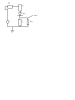
Photo's:

Top 1.jpg

Bottom 1.jpg


Pink wire attached to neg leg of big cap

Please help
 

WHONOES

May 20, 2017
1,217
Joined
May 20, 2017
Messages
1,217
The gate of the FET should have a square wave signal on it. If not, the drive circuit or the FET has failed. If you have access to an oscilloscope, remove the FET and see if there is a signal on the gate pad.

Take care when poking around on a board like this as the voltages present at lethal.
 

bushtech

Sep 13, 2016
1,025
Joined
Sep 13, 2016
Messages
1,025
Thanks whonoes. I am being very careful here, also running the device via a 60W globe. Sadly I don't have a scope so anything else I can check?
 

WHONOES

May 20, 2017
1,217
Joined
May 20, 2017
Messages
1,217
You could in the first instance try replacing the FET and see what happens. Also, as a bit of an after thought, is there a resistor in series with the FET gate?
 

bushtech

Sep 13, 2016
1,025
Joined
Sep 13, 2016
Messages
1,025
Had to hunt to find something connected to the gate

Bottom 2.jpg
 

bushtech

Sep 13, 2016
1,025
Joined
Sep 13, 2016
Messages
1,025
The only thing I can reliably see on that transistor(?) is 2F
 

WHONOES

May 20, 2017
1,217
Joined
May 20, 2017
Messages
1,217
The 2F mark is smd shorthand for variations on the old 2N2907A but in a SOT-23 package. The ones I have found are FMMT2907A. KST2907A and MMBT2907A.
You could try replacing that for a start.
My preferred method for removing such devices is to cut through the legs as close to the body of the device as you can, using a very sharp scalpel whilst applying pressure to the top with a pointed object such as a scriber. It is then easy to wipe the pin remnants off the pads using your soldering iron.
 

WHONOES

May 20, 2017
1,217
Joined
May 20, 2017
Messages
1,217
336V on the drain suggests your mains is about 237V. I that correct?
Let us know how you get on.
 

bushtech

Sep 13, 2016
1,025
Joined
Sep 13, 2016
Messages
1,025
Yep, 238V here. I get 336V on the big cap but 400V on the drain of the 2F
 

73's de Edd

Aug 21, 2015
3,622
Joined
Aug 21, 2015
Messages
3,622
Sir Bushtech . . . . .

Just to the 10 o'clock position of your complementary pair of driver transistors for your POWER FET, should be the 8 pin integrated circuit, minus its one pin pulled for board gap HV isolation .
It is being the brains of the control unit for the HOT chassis side .
Can I get its identifying numbering ?

Am I correct that this unit shows no shorted or BLOWN diodes or semis on the unit on the COLD side of the supply, which is being all circuitry to the right side of the boards central op-trick-all i-so-fum-u-lator, with the unit probably having gradually died due to progressive E-capacitor atrophy.

Also, do I remember you having a cap analyzer that has ESR capability ?
If so, check out your Post #1's very top photo and find the round reddish brown FI for a landmark reference and test the two smaller E caps that are being located just to the right.

Aside . . . .
How come . . . I suspicion that unit puts out a whole 1 amp of car battery trickle charging capability.


73's de Edd
.....
 

bushtech

Sep 13, 2016
1,025
Joined
Sep 13, 2016
Messages
1,025
Thank you for coming in 73's de Edd. Unfortunately the nice CTEK people, in addition to not publishing schematics/ wiring diagrams, have also removed markings from some components, the 8-1 pin IC being one of them.

Correct, I can see no blown or damaged components on the cold side

Nothing wrong with your memory, I had an ESR tester which didn't survive checking a charged cap (duh) New one has been ordered and has been sitting at our Post Office which is on strike so nothing forthcoming. Otherwise they would have been the first things to check

Not sure what it trickle charges at but it can do 3.8A charging
 

bushtech

Sep 13, 2016
1,025
Joined
Sep 13, 2016
Messages
1,025
@WHONOES: When checking voltages on the 04N60C3 heatsinked mosfet should I be on AC or DC? Measurements were done on DC
 

WHONOES

May 20, 2017
1,217
Joined
May 20, 2017
Messages
1,217
If the FET is being switched, which it probably isn't otherwise the unit would likely be working, you should be on ac. Having said that, you probably wouldn't see anything as the gate signal will be at several tens of KHz which your meter won't be able to resolve.
You could make a simple detector to do the job. See the attachment below.
V1 in the diagram would be the Gate Source pins of your FET and R2 is representative of the input impedance of your DMM. Connect DMM as indicated.
You can then use your DMM switched to dc. You should be able to measure a voltage in the range of 2 to 10V I should imagine. Zero means there is no signal.
 

Attachments

  • Detector.pdf
    8.4 KB · Views: 42

bushtech

Sep 13, 2016
1,025
Joined
Sep 13, 2016
Messages
1,025
Thanks a million WHONOES. I do want to build this circuit. BTW, can this circuit be used to check mosfets in SMPS like a PC power supply?

My electronics knowledge and experience is still quite limited. As such, I am struggling to get my head around this one.
Coupla questions:

1. The one side of V1 is connected to the gate and the other to the source of the MOSFET. Correct?
2. Is the earth (Ground? next to V1 connected to something like the neg leg of the big cap?
3. How is the DMM connected. DMM has 2 probes and one connection on circuit. I don't understand how to connect the DMM.

I have redrawn your circuit in MS Paint and attached it. Might make it easier for you if you want to show something different on the schematic

Thanks again
 

Attachments

  • Detector.png
    Detector.png
    23.2 KB · Views: 26

WHONOES

May 20, 2017
1,217
Joined
May 20, 2017
Messages
1,217
See picture below. Hope that helps. Apologies for the stylised FET.
Come back if you are still having difficulties.
 

Attachments

  • detector.jpg
    detector.jpg
    34.5 KB · Views: 31

bushtech

Sep 13, 2016
1,025
Joined
Sep 13, 2016
Messages
1,025
Thanks WHONOES

Should be able to crack it with the sketch.

Just a question from my previous post: "BTW, can this circuit be used to check mosfets in SMPS like a PC power supply?"

ie is this faily generic?
 

WHONOES

May 20, 2017
1,217
Joined
May 20, 2017
Messages
1,217
Sorry forgot to reply to that bit. Yes. But beware the little detector does have limitations.

Edit:
Forgot to mention, the circuit should be floating hence, no ground symbol on the sketch.
 

bushtech

Sep 13, 2016
1,025
Joined
Sep 13, 2016
Messages
1,025
Oooh! Thanks for the floating circuit bit of info. Busy getting SMPS into my old brain. Was getting mighty confused with them until I realised hot and cold side of SMPS have two different ground points lol.

Postal strike here seems to have ended, so there's hope. I don't have either of the caps. For the 1nf cap will a 1kV ceramic do?

100mf seems to a bit of a problem. 10V probably too low and 400V snap in pricey

http://www.mantech.co.za/Stock.aspx?Query=cap+100mfand
 

WHONOES

May 20, 2017
1,217
Joined
May 20, 2017
Messages
1,217
Hi again. The 100mF you quote should be 100nF. I blame my poor hand writing for the confusion
For the 1nF, anything over 50V would do. Ceramic is fine. The same goes for the 100nF.
Sorry for the confusion.
 
Top