Maker Pro
Maker Pro

SIPO shift register. How to read data?

NotoriousRampage

Mar 17, 2012
3
Joined
Mar 17, 2012
Messages
3
Hey guys ,
I'm new here. I'm working on a CAN-Bus project. I'm stuck at designing a SIPO shift register, particularly at getting the stored bits out of the D-FF. Can anyone help? I've been googling for about 3 hours now , but to no avail.
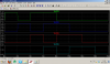
Let's just say I'm designing a 4 bit shift register. The outputs should be available after 4 clock cycles. How to read the data non-destructively?
Thanks in advance

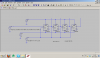
P.S.: I'm using LTSpice for my design. Should you require the schematic, let me know.
 

(*steve*)

¡sǝpodᴉʇuɐ ǝɥʇ ɹɐǝɥd
Moderator
Jan 21, 2010
25,510
Joined
Jan 21, 2010
Messages
25,510
If the shift register is SIPO then all the bits are already available at the outputs.

If it's a serial output you're after then I guess you can read the last parallel output and clock the bits through it.

If you want to do this non-destructively then simply couple the serial output to the serial input so the bits roll through the register.

If you connect them using a resistor then a normal serial input will be able to override the loopback, but it will require the logic driving it to ho high impedance while you're reading out the data serially. An alternative is some logic so you can select one source or the other as the input of the shift register.

An even easier way is to monitor the first output as you clock the data in, or even monitor the input as you clock the data in, but I guess you want to be able to clock the data out after some random delay, not with a one clock cycle delay :)
 

NotoriousRampage

Mar 17, 2012
3
Joined
Mar 17, 2012
Messages
3
Hey Steve,

thanks a lot for your he, it was very helpful. Unfortunately, I still don't get how the parallel outputs of a shift register are available simultaneously, since the transient simulation in LTspice shows that the outputs are only available between 6us and 8us. The clock period is 2us. The flip flops in use are 74HC74.

Here are some screen shots for more information.
Top graph represents the 1st FF output on the left and the last the output of the fourth.
 

Attachments

  • schematic.png
    schematic.png
    38.1 KB · Views: 2,679
  • simulation.png
    simulation.png
    42.6 KB · Views: 707

(*steve*)

¡sǝpodᴉʇuɐ ǝɥʇ ɹɐǝɥd
Moderator
Jan 21, 2010
25,510
Joined
Jan 21, 2010
Messages
25,510
That's how a shift register works. If you keep on clocking it after you shift in the data, it shifts right back out again.

If you stop the clock after the 4 data bits have been clocked in (after 4 clock cycles) the parallel outputs will have the 4 bits on them.
 

NotoriousRampage

Mar 17, 2012
3
Joined
Mar 17, 2012
Messages
3
That's how a shift register works. If you keep on clocking it after you shift in the data, it shifts right back out again.

If you stop the clock after the 4 data bits have been clocked in (after 4 clock cycles) the parallel outputs will have the 4 bits on them.

I see . That makes sense. Thanks a lot for your help.
 
Top