Maker Pro
Maker Pro

Power supply dead. Pictures inside... repairable?

dmul

Dec 2, 2016
3
Joined
Dec 2, 2016
Messages
3
Hi all. Hopefully someone here can help advise me on this issue.

I have an iPod/music player called a Bowers & Wilkins 'Zeppelin air' that stopped working a while ago. Zero power to the unit despite fuses and external supply being good.

The power supply board in the unit is known to be the fault with these devices. So I removed the board to see if I could find any blown capacitors.

I found none, all looked in good order so I flipped the board and saw what looks like a burned out IC chip?

Is this board dead or fixable at all?

The manufacturing company wont sell a new power board, they want the unit in (at cost) to repair. I would just like to put my mind at ease that there is nothing I can do before sending it back.


Pictures below, thank you for looking :)
Dave

Top side of power supply board, all looks OK.

O3XV6fC.jpg


Bottom side... and close ups of the chip I spotted...

6yQI2JE.jpg


EKzl8pZ.jpg


3lv6d2e.jpg
 

73's de Edd

Aug 21, 2015
3,622
Joined
Aug 21, 2015
Messages
3,622
.

Sir dmul . . . .


Too wide of a pad for this boards dedicated diode layout protocol.
Under all of the smoky carbonization I am reading that as R31 which is a 0.5 ohm SM resistor.
I think that a nearby connectivity related transient problem resulted in a power semi blow up that then, additionally, took out that resistor.
You gave us a GOOD component side shot of the board, can you now do an equally well lighted and in focus shot of the WHOLE foil side of the board.
With it just filling up the whole pic frame and the board being squared up in the frame and no parallax error.

Note that adjunct to ceramic chip capacitor C39 at either of its ends, a short distance away, that there are some pad soldered component leads . . . particularly the one beside T4 unit . . . that looks like having evolved into a floating lead and an arced away connection has developed.


73s de Edd
 
Last edited:

dmul

Dec 2, 2016
3
Joined
Dec 2, 2016
Messages
3
Hi 73's de Edd. Thanks for your reply. Here is a full clear high res shot of the secondary side.

I took another shot of the component side, with the board just flipped to the right.

C4yK67A.jpg


NXKrTKW.jpg
 

dmul

Dec 2, 2016
3
Joined
Dec 2, 2016
Messages
3
.

Note that adjunct to ceramic chip capacitor C39 at either of its ends, a short distance away, that there are some pad soldered component leads . . . particularly the one beside T4 unit . . . that looks like having evolved into a floating lead and an arced away connection has developed.

Do you mean the pad soldered point here just above T4?

0T8yVv3.png


If so, thats one of the leads from the transformer wrapped in yellow on the component side.
 

the great potato

Dec 2, 2016
52
Joined
Dec 2, 2016
Messages
52
im sure it can be fixed, but most likely something eles went bad that blew that component, ive never personally replaced a transformer, but that may be the problem since the lead traces back to it. not to mention that damage looks caused by a good jolt, judging by the damage. But yes im sure it could be fixed, but sadly finding that chip and actualy soldering it in is the challenge. Have you tried ebay to see if you can find that board to replace ? Replacing the board seems more feasible, to me at least.
 
Last edited:

the great potato

Dec 2, 2016
52
Joined
Dec 2, 2016
Messages
52
well im not seeing that board on ebay, searching with the Serial number at least. But not all hope is lost you can prob track it down.
 

davenn

Moderator
Sep 5, 2009
14,260
Joined
Sep 5, 2009
Messages
14,260
Do you mean the pad soldered point here just above T4?

0T8yVv3.png


If so, thats one of the leads from the transformer wrapped in yellow on the component side.


give a larger pic of this section VERY VERY clear and sharp ... lets see if we can make out that damaged resistor value

VERY gently clean up the top of the resistor with a damp cotton bud and lets see of the 3 digits can be read

it may be that that resistor is the only problem but it may be that it failed because of a component failure elsewhere
 

73's de Edd

Aug 21, 2015
3,622
Joined
Aug 21, 2015
Messages
3,622
.

Sir dmul . . . . . . .

Those two connections, being of particular interest, are the primary of the SMPS power transformer, and if in flow soldering manufacture, were not FULLY solder wetted, progressive high current intensity at
those junctions could have created a progressive heating and cratering of a joint (example shown within inset) and then an initial arcing and its related voltage transients could have crunched either of its
two driver TO-220 cased power semiconductors that I have YELLOW rectangles marking up.

Need to know the marked on IDs of those items as well as their driver IC U4 down below. Also throw in PINK marked semis.

The heated foil of one lead off from D2, may also designate it being faulty. . . . . unless caused by being collateral heating of R31.

Also check for any cratering of the leads of the YELLOW rectangled units.

Do you know how to test semi junctions, using a DVM in its diode test mode ?
Also, can you take said meter and switch to conventional LOW OHMS mode and short together your test probes to take a reading of combined lead resistance . . . commit to memory . . . then measure
the R31 value and extract your test lead resistance error, to see how close its current value comes to its original one half of an ohm of resistance .

EXTRACTED REFERENCE SNIPPET MARKUP:

Football_Power_Supply.jpg


73's deEdd
 

cjdelphi

Oct 26, 2011
1,166
Joined
Oct 26, 2011
Messages
1,166
The damage looks like psychical damage not so much something went wrong

How did the copper track get exposed like that? It's like something metal was just jammed in there causing a short.
 

73's de Edd

Aug 21, 2015
3,622
Joined
Aug 21, 2015
Messages
3,622
CJD
et al . . . . .
The rest of the story . . . . .

The inset photoreference is the initial condition of the PCB in the affected area.
A request for a total board shot of the foil side of the board ADDITIONALLY resulted in a much appreciated freebie, of a mechanico / chemical clean up of the subject area before the new photo..
A look over in the adjunct R28-R29-D8 area reveals the pristine condition of the factory new conformally coated board.
A closer look at the the inset photo reveals the bubbled, peeling, blistered and burnt condition of the R31 damage epicenter.
In addition to the chemical cleaning, the use of a screwdriver tip ? knife ? scribe ? resulted in 7 or so scarring marks / surface scratches and the flipping off, of a bit of BOTH conformal coating hardened " slag " AND some etch resist coating . . . . .with a small bare copper foil area as a resultant..

An inclusive . . . .Sir dmul . . . . query .

At the bottom mentioned connection of the main SMPS primary bottom solder pad . . .just above Transistor 4 symbolization . . . do we have a created wire " floater" connection, or is it just being a lighting / shadow optical collusion / confusion ?

BEFORE and AFTER

Inset PCBs.jpg

73's de Edd
 
Last edited by a moderator:

KolfMAKER

Oct 31, 2022
1
Joined
Oct 31, 2022
Messages
1
I am working on a Bowers & Wilkins as well: a Zeppelin Air and an A7. They are notorious for the type of issues described in this thread.

At this time I need to replace several SMD components. But it would be very helpful for the overall repair to have a PCB-components list.

Does anyone have that?
Please share.
 
Last edited:

corado

Jan 4, 2023
2
Joined
Jan 4, 2023
Messages
2
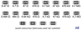
The Resistor valueR31 is R50(0,5 Ohm)

Has anyone found the failure?
I habve the same here, but no optcal damage, mabe two Diodes, because the show 0V, but I have to solder them out later and test it outside
 
Last edited:

bertus

Moderator
Nov 8, 2019
3,321
Joined
Nov 8, 2019
Messages
3,321
Hello,

R50 is likely 0.50 Ohms.
smdresistor.jpg
Bertus
 
Top