Maker Pro
Maker Pro

n-mosfet replacement on Qnix lcd monitor

AMT

Jan 28, 2016
19
Joined
Jan 28, 2016
Messages
19
Hello again,

So recently I dug out a rather nice 1440p Qnix monitor that had gone kaput a while back and never got around to sending back to the manufacturer for a replacement. I decided to message the merchant, and they said that if I want to I can attempt to fix it myself, and in the event I cannot, they will provide me with a replacement (so long as I ship the old one back) even though the monitor is long past warranty (I bought it in 2013) so win-win right?

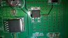
Problem is, I cannot identify the n-mosfet on the board. I found another fellow on another forum who had asked a similar question, but given that he only has two posts and hasn't had any activity on the forum since November I am doubtful I will here back from him.

I am hoping somebody here can point me in the direction of a suitable replacement part, as it should be a relatively easy fix (assuming it is only the visible damage I have to worry about). The part is marked as 540N 3811G.

The provided picture is taken from the other thread as mine is the exact same board, same part, same place, same damage.

Thanks again people, very helpful community here and I really appreciate all of the help I can get.
 

Attachments

  • Oq7Jj.jpg
    Oq7Jj.jpg
    88.4 KB · Views: 398

73's de Edd

Aug 21, 2015
3,628
Joined
Aug 21, 2015
Messages
3,628
Sir AMT . . . . .

Looks like you might need yourself an IRF 540 in a D pak casing.

http://www.mouser.com/Semiconductor...ET/_/N-ax1sf?P=1yzorz4&Keyword=IRF540&FS=True
( Its a golden oldie . . .even obsolete . . .for new design . . .but more 'spensive than your others)

Look at the Infineons at the bottom, as they don't have the two side cutouts, like the old units had, plus give us the measurements across the width of your unit.
It might be another casing variant, if that 5 leaded IC to the left ( FAC2596 ) is having the same case size as a conventional TO-220.

73's de Edd


.
 
Last edited:

Alec_t

Jul 7, 2015
3,591
Joined
Jul 7, 2015
Messages
3,591
I think I'd be tempted to look for a FET with a lower Rds(on) rating, since the same failure in two monitors indicates the FET is under-specified.
 
  • Like
Reactions: AMT

AMT

Jan 28, 2016
19
Joined
Jan 28, 2016
Messages
19
Sir AMT . . . . .

Looks like you might need yourself an IRF 540 in a D pak casing.

Thank you again kind Sir! Without your expertise I would be throwing these very serviceable items in the junk pile, or paying out the wazoo to have them repaired!
:)

Look at the Infineons at the bottom, as they don't have the two side cutouts, like the old units had, plus give us the measurements across the width of your unit.
It might be another casing variant, if that 5 leaded IC to the left ( FAC2596 ) is having the same case size as a conventional TO-220.

73's de Edd


.
My calipers tell me the width is 0.252 in.
Edit: I should mention my calipers are not the best, so that reading may very well be a bit off.

I think I'd be tempted to look for a FET with a lower Rds(on) rating, since the same failure in two monitors indicates the FET is under-specified.

I was thinking along similar lines.

73's de Edd, could you point me towards a more viable replacement?

:)


Edit: I found another device with a similarly sized n-mosfet labelled APM3055L WJ15P.
Would that work as a replacement?
 
Last edited:

AMT

Jan 28, 2016
19
Joined
Jan 28, 2016
Messages
19
Apologies guys, I hope I haven't offended anybody.
My electronics knowledge is quite limited. Though I can solder and desolder relatively decent.

If I can replace the parts I need with parts I have, it would be awesome to get this thing working without having to order something, but either way! :D
 

73's de Edd

Aug 21, 2015
3,628
Joined
Aug 21, 2015
Messages
3,628
.


Sir AMT . . . . . .whooooops . . . my lysdexia almost made your name into a cash withdrawal machine !

You sez:

Edit: I found another device with a similarly sized n-mosfet labelled APM3055L WJ15P.

That number given above specs out as being "less" of a part than is presently in the unit.

Funny that they used the "root number " of a "universally used / familiar" power bipolar transistor, having been used in multi past decades in their assigned
numbering of their device . . . . to wit . . . ."3055".

You say:

Problem is, I cannot identify the n-mosfet on the board.

I am hoping somebody here can point me in the direction of a suitable replacement part, as it should be a relatively easy fix

(assuming it is only the visible damage I have to worry about).


If that is your units photo, are you condemning the semiconductor, just because it inherently runs hot and that the board has eventually discolored a bit

underneath it ?

Has the Pwr CMOS unit actually been tested ohmically and has a voltage test been conducted across its drain and source ?.

I find nil available on that Qnix unit in the way of schematics, but I can "read the board" and see that is being the principal power

element of a buck power supply.

I'm using a photo that shows the complete board and marking up its adjunct functions, in our particular area of interest.

Feed us back the voltage and current specs of the units separate "wall wart " type of external power block that plugs in to my

marked power connector.

Techno - File:

pmsgWFj.jpg


73's de Edd

.
 

AMT

Jan 28, 2016
19
Joined
Jan 28, 2016
Messages
19
Hello. No, the picture of the board is not my board per se, as it is not my picture. But it is the same type of board and the damage is in the same place (which suggests, it would seem, that I am not the only one with the problem). :)
The mosfet in the picture is leaking and the monitor no longer turns on. This happened after plugging it in one day and a popping sound occurring (and a burning electronics smell emitting). Upon disassemble and inspection the only visible damage that could be seen is that of the mosfet in question. It may very well be that there is other damage in other places on the board, but I lack the necessary tools to test the board (my multi-meter is not operative at the moment) but I suspect the replacement should do what I am hoping, and in the event it does not, at least I am getting some practice. :D

I did notice after my message and after finding the datasheet for the apm3055l (I know absolutely nothing about designations and naming conventions at this point) that indeed it is rated for 30v, while the previous (damage) part is much higher than that.

Again, I am treading new ground here so if I sound like I don't have a clue what I am talking about it is because I likely do not. I am, however, eager to learn whatever I can from this so I hope you can bear with me as I take my first "baby steps" into this strange new territory. (lol).

The power adapter reads thusly:
MODEL: M120500P911
INPUT: 100-240V~50/60Hz 1.2A
OUTPUT: 12V
(3 dashes with line symbol, so DC) 5000mA


I hope that helps. :D


Edit: I feel that I should mention that this particular monitor is Korean. The writing on the power brick is Korean and it is manufactured in that Country, though it is marketed and sold here in NA.

Another Edit: Apparently the mosfet issue is much more common than I initially realized.

Also: http://www.overclock.net/t/1471025/...onitors-bought-online-how-long-did-it-last/20
 
Last edited:

73's de Edd

Aug 21, 2015
3,628
Joined
Aug 21, 2015
Messages
3,628
.

Sir AMT . . . . . .


I had marked up the board with all of the parts in its portion that is being associated with its on board power supply section and you are apparently experiencing a failure with.

The two things that I did not mark up are at the left center side of the board and almost being to the connector to the left that has multiple white wires and one red marker wire.
Those are two brown rectangular monolithic block ceramic capacitors and perform the filtering of that supply, they do not have high enough value of capacitance and filtering results to provide a pure-pure DC voltage output like might be needed in other circuitry..

Which is really not all of that importance, since this supply is used for the powering of LED light banks to back light your frontal LCD panel.

Those LED lights illuminate up for frontal light passage, along with a multiplexed selective pixel activation on the frontal LCD panel, to create your monitors front display.

To confirm your monitors situation, and its type of failure, as is being related to this power supplys failure . . . . .

Go down the list and refer to, and perform my testing procedure, as is being explained in my post #9 .


https://www.electronicspoint.com/threads/how-do-i-repair-my-monitor.277189/#post-1679473

As for the different options on the N channel power mosfet:
The lower the on resistance (Rds on) in the FET's drain to source conductive, path the less power will be dissipated in that device.

I am still sorting thru the myriad of possibilities for a better choice of a N channel logic level drive power MOSFET for the ? able one being in your unit now.


73's de Edd


.
 

AMT

Jan 28, 2016
19
Joined
Jan 28, 2016
Messages
19
.

Sir AMT . . . . . .


I had marked up the board with all of the parts in its portion that is being associated with its on board power supply section and you are apparently experiencing a failure with.

The two things that I did not mark up are at the left center side of the board and almost being to the connector to the left that has multiple white wires and one red marker wire.
Those are two brown rectangular monolithic block ceramic capacitors and perform the filtering of that supply, they do not have high enough value of capacitance and filtering results to provide a pure-pure DC voltage output like might be needed in other circuitry..

Which is really not all of that importance, since this supply is used for the powering of LED light banks to back light your frontal LCD panel.

Those LED lights illuminate up for frontal light passage, along with a multiplexed selective pixel activation on the frontal LCD panel, to create your monitors front display.

To confirm your monitors situation, and its type of failure, as is being related to this power supplys failure . . . . .

Go down the list and refer to, and perform my testing procedure, as is being explained in my post #9 .


https://www.electronicspoint.com/threads/how-do-i-repair-my-monitor.277189/#post-1679473

As for the different options on the N channel power mosfet:
The lower the on resistance (Rds on) in the FET's drain to source conductive, path the less power will be dissipated in that device.

I am still sorting thru the myriad of possibilities for a better choice of a N channel logic level drive power MOSFET for the ? able one being in your unit now.


73's de Edd


.

Hello Sir,

While I appreciate the capacity to assist me in my endeavor, there is no longer that need. I purchased the mosfet mentioned by alec_t in this thread, and in the process of repair I, in my ignorance, heated it up too much and peeled off a large piece of the board trace along with it.

The board is now being replaced by the manufacturer, for a cost. :/

Ah well, at least I tried. I did learn though! After messing up that particular job, I continued to practice (I have a large amount of various boards laying around the house to play with) and now I am quite confident that the next time I need to replace a mosfet, or similar on board item, I will do so quite well.

:D
 

73's de Edd

Aug 21, 2015
3,628
Joined
Aug 21, 2015
Messages
3,628
.


I believe that I can tell you exactly how to correct your problem you created with the PCB foil delamination..
As you can see, that whole quarter section of the pcboard has its foil left on it, to serve as a heat sink to carry the heat away from that/THE power CMOS that has its tab soldered directly to it
How about telling me the dimensions/area of the foil tab that was pulled from the board.
Then I will tell you a successful install procedure for the new part.

73's de Edd

.
 

AMT

Jan 28, 2016
19
Joined
Jan 28, 2016
Messages
19
.


I believe that I can tell you exactly how to correct your problem you created with the PCB foil delamination..
As you can see, that whole quarter section of the pcboard has its foil left on it, to serve as a heat sink to carry the heat away from that/THE power CMOS that has its tab soldered directly to it
How about telling me the dimensions/area of the foil tab that was pulled from the board.
Then I will tell you a successful install procedure for the new part.

73's de Edd

.
I will take a picture of the area and show you. It is a quarter inch area around the old n-mosfet that lifted up.
 

AMT

Jan 28, 2016
19
Joined
Jan 28, 2016
Messages
19
Ok, here is the pictures. You can't really see all to well, but that there is the new mosfet (not sure if I ruined it in the process) and you can kind of see a darker area where the board peeled up along the sides of it, and to the beginning of that third row of little holes in groups of four.

new2.jpg new3.jpg new4.jpg new1.jpg
 

Alec_t

Jul 7, 2015
3,591
Joined
Jul 7, 2015
Messages
3,591
It looks well and truly cooked :(. Unfortunately the copper pad on the board is relied on for conducting heat away from the FET. If you can remove the green protective pcb coating in that region you may be able to attach a new pad to the board, made from a bit of thin copper sheet.
 

AMT

Jan 28, 2016
19
Joined
Jan 28, 2016
Messages
19
Hmmmm.... I still have another replacement n-mosfet. I could remove that one and try again.

Are they supposed to connect on the sides and/or the front as well? Or is it only the two pins on the back that are important?
 

Alec_t

Jul 7, 2015
3,591
Joined
Jul 7, 2015
Messages
3,591
The two pins at the 'back' are gate and source. The bigger tab is the drain. So all 3 are important! But the biggger tab also plays a big part in conducting heat away from the FET.
 

AMT

Jan 28, 2016
19
Joined
Jan 28, 2016
Messages
19
Hmmm, ok. So the big tab is kind of like a heatsink then.

I noticed when I lifted the old FET that the entire area below it seemed conductive?

Do you think it would be feasible for me to remove this one and replace it again and make it work? Or am I SOL if that part of the board had peeled up?
 

73's de Edd

Aug 21, 2015
3,628
Joined
Aug 21, 2015
Messages
3,628
.

Sir . . . . . .ATM

Cramped for time now . . . .but rosin flux up the two small gate and source tabs and lift them up free of their solder pads at the board.
Now, to remove that larger drain tab, also wet its big tab down with rosin flux and check to see that your . . . .hopefully . .50 watt irons soldering tip is completely tinned and shiny.
Inspect the surface mount diode to the right to see if it will be in the way of your soldering irons manipulation. If so hold off til I tell you how to safely pull it.
Your best friends now are going to be rosin flux and solder blobs.
You are needing to get a lot of heat to that copper tab, so instead of the very tip of that iron , use the well tinned area of the tiplet just down to its side so that more heat can be transferred in from a wider application area.
Initially, go in to that fluxed drain tab and initially use the tips side to get a big blob (B-B size)of solder adhering to the left end of the tab and then move to the right end of the tab and get a big blob adhering there. Then the final move is to the center and get a blob there.
Now you rapidly get your irons tiplets side continuously moving between the 3 blobs and all three will be constantly molten and flow together and transfer all their heat and the solder will wick and migrate down to the old solder bond between the PCB foil and the drain tab.
Your left hand has a pair of conventional slip joint pliers, opened up to its second position, such that you are gripping across the transistors top epoxy case and additionally placing a right or left rotational twist /tension on the transistor.
At a critical heat level, the transistor should rotate free as the last solder bonding has melted and then you extract with a fast rotational lift.
Clean up the board with solder wick, with a lot more of that rosin flux to enhance its effectiveness in solder absorption.
Then clean up that affected board area with alcohol and do a final check to see how well the folded foil can be pressed back down to its initial PCB surface .
The copper is so malleable, that the butt end of a metal exacto knife holder, in using a side to side downward pressure / movement should press away all of its wrinkles, so that it might then go all the way down flat again.
Use a #11 Exacto knife blade to cut away what little copper that would not flatten down.


Waiting for questions or progress or hangups.

Then info will come forth for foil repair and PROPER preliminary prep of another transistor for installation and then its actual install.

73's de Edd


.


.
 

AMT

Jan 28, 2016
19
Joined
Jan 28, 2016
Messages
19
Ok, thanks. Cramped for time as well so I will get to it in the evening (it is 1 pm here now) and get back to you then.
 

AMT

Jan 28, 2016
19
Joined
Jan 28, 2016
Messages
19
Ok, so I ended up purchasing a replacement board from the vendor (warranty was long since expired) and within a week the exact same issue.
I went ahead and purchased more of the
STD70N10F4
that Alec_t linked above, and this time the replacement went extremely well (I'm actually quite proud of myself). Now, unfortunately, I got the board re-installed and fired up the monitor, and everything worked perfectly well, for about 5 minutes and I started to hear buzzing and the smoking started again (o_O).
I checked the board and it is **the same mosfet** that has burned out.

I do have more replacements and am now quite comfortable switching them out, but would like to figure out what may potentially be going wrong before I bother to put another one through its paces.

Is it possible (or even probable) that if the drain tab isn't soldered on 100% right (I can't see how it wouldn't be, but there appears to be a micro gap about a fraction of a millimeter big between the bottom of the part and the pad on the PCB) that would cause it to go?

Is it possible as well that the powerbrick they are supplying is too much for the board to handle when using NA designated electrical outlet?

I am so close to getting this thing fixed and have you guys to thank for it, here is hoping you can help me figure this out!! :)
 
Top