BlackMelon
- Aug 7, 2012
- 188
- Joined
- Aug 7, 2012
- Messages
- 188
Hello,
Right now I'm doin a gate driving hobby.... My target is to replace the gate driver with some appropriate discrete components (Of course, I don't want it to be as perfect as the commercial gate driver but not so lousy)
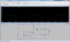
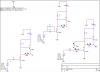
As the circuit shown in the picture, I want to know that why the voltage signal at Q(A)'s collector is so ugly?.... (I saw this from an oscilloscope), I've tried to reduce gain to get a higher bandwidth by reducing the its collector resistance.. but it helps just a little bit.....
PS: Voltage at Q(B) shown some capacitor charging in the rising edge but it doesn't distort the signal from the square wave so much
PS2: The MOSFET gate signal has some parts similar to the Q(A)'s collector.... some is similar to the Q(B)'s collector to... I guest it's the summation of the two signal.
(The circuit is redesigned from http://tahmidmc.blogspot.com/2012/12/low-side-mosfet-drive-circuits-and_23.html)
BlackMelon
Right now I'm doin a gate driving hobby.... My target is to replace the gate driver with some appropriate discrete components (Of course, I don't want it to be as perfect as the commercial gate driver but not so lousy)
As the circuit shown in the picture, I want to know that why the voltage signal at Q(A)'s collector is so ugly?.... (I saw this from an oscilloscope), I've tried to reduce gain to get a higher bandwidth by reducing the its collector resistance.. but it helps just a little bit.....
PS: Voltage at Q(B) shown some capacitor charging in the rising edge but it doesn't distort the signal from the square wave so much
PS2: The MOSFET gate signal has some parts similar to the Q(A)'s collector.... some is similar to the Q(B)'s collector to... I guest it's the summation of the two signal.
(The circuit is redesigned from http://tahmidmc.blogspot.com/2012/12/low-side-mosfet-drive-circuits-and_23.html)
BlackMelon
")