BlackMelon
- Aug 7, 2012
- 188
- Joined
- Aug 7, 2012
- Messages
- 188
Hello,
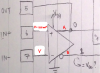
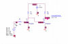
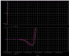
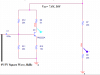
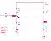
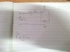
My IC takes in a square wave input as written on the attachment. I want to apply that input and measure the current, so I will be able to determine the input resistance value. However, my multimeter is not a true RMS one. As what I know, the RMS current is accurate only if it is in a sinusoidal waveform. So, can I apply the ripple waveform shown on the attachment?
Thank You
Ps. My IC is HIP4080A, a mosfet driver. The input pin is "HEN".
")