Hello,
This post is long but simple…….it just concerns redesign of a Switch Mode LED Driver and a potential problem brought about due to increased flux excursion in the new inductor.
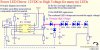
Our design contractors have designed for us a Boost converter LED driver of the following spec:-
V(in) = 12V
I(out) = 450mA
(-but LEDs are in parallel so each individual LED current is 150mA)
V(out) max = 33V
Continuous conduction mode
Switching frequency = 983KHz.
PCB size = 11mm by 50mm
PCB = double sided.
PCB is potted into a cyclindrical moulding.
The LEDs are in series strings of 8 LEDs, and there are three of these in parallel. (24 LEDs in total)
The LEDs are Advanced Power TopLEDs (LB G6SP) by osram-os
LED datasheet:-
http://catalog.osram-os.com/catalog...Oid=000000020000fa02005e0023&act=showBookmark
LPS6225-103ML inductor datasheet
http://www.coilcraft.com/pdf_viewer/showpdf.cfm?f=pdf_store:lps6225.pdf
Each LED string has a 10R, 1206 resistor in series with it to equalise the parallel LED currents.
Unfortunately , each 1206 resistor dissipates 225mW even when the LED currents are perfectly matched…….if the LED currents become more mismatched then these resistors are going to be seriously over-stressed. (over-powered)
Therefore,
We wish to re-design this boost converter with all the LEDs in series, and throw away the series 10R resistors.
This means, the new spec becomes:
V(in) = 12V
I(out) = 150mA
V(out) max = 100V
(Obviously we must use a different control chip because the LT3477’s internal FET is only rated to 42V.)
Now the problem comes because we can not now use continuous conduction mode. This is because the duty cycle would be 0.88, and almost all control chips won’t provide a duty cycle that high. Some controllers will provide that high duty cycle, but their internal slope compensation is not sufficient to be able to handle that high duty cycle.
-We could use an external slope compensation network, but external slope compensation networks do not work well at high frequency (we need to use high switching frequency due to the small PCB size)
-We could use a voltage mode chip, but unfortunately there are very few of these about (there is UCC35705, but it has no on-chip FET driver, and no internal error amplifier).
Anyway, we therefore have decided to use a discontinuous mode boost converter to do it.
The current peak is obviously higher for DCM boost, and this means that the flux excursion will be greater in the inductor, ……….and since we have to operate at high frequency, we are worried about the inductor overheating.
We have decided to use Coilcraft XAL6060-103ME , 10uH inductor
XAL6060-103ME inductor datasheet:
http://www.coilcraft.com/pdf_viewer/showpdf.cfm?f=pdf_store:xal60xx.pdf
We have dropped the switching frequency down to 295 KHz, to try and keep the inductor cool (inductor core loss)…but as you can note, its still a high switching frequency.
However, the core loss calculator on the coilcraft website tells us that it cannot calculate our core loss because our inductor’s peak current (3.07A) is more than 50% above the inductor’s RMS current (1.62A).
The inductor datasheet does not tell us what type of ferrite is used, and there are no core loss curves, therefore we have no way of knowing what the core loss will be……we have only one option…..to build it and test it and measure inductor temperature……but this will be expensive if it fails.
Anyway, do you think that this XAL6060-103ME inductor will suffer massive core loss in our DCM Boost application?
This post is long but simple…….it just concerns redesign of a Switch Mode LED Driver and a potential problem brought about due to increased flux excursion in the new inductor.
Our design contractors have designed for us a Boost converter LED driver of the following spec:-
V(in) = 12V
I(out) = 450mA
(-but LEDs are in parallel so each individual LED current is 150mA)
V(out) max = 33V
Continuous conduction mode
Switching frequency = 983KHz.
PCB size = 11mm by 50mm
PCB = double sided.
PCB is potted into a cyclindrical moulding.
The LEDs are in series strings of 8 LEDs, and there are three of these in parallel. (24 LEDs in total)
The LEDs are Advanced Power TopLEDs (LB G6SP) by osram-os
LED datasheet:-
http://catalog.osram-os.com/catalog...Oid=000000020000fa02005e0023&act=showBookmark
LPS6225-103ML inductor datasheet
http://www.coilcraft.com/pdf_viewer/showpdf.cfm?f=pdf_store:lps6225.pdf
Each LED string has a 10R, 1206 resistor in series with it to equalise the parallel LED currents.
Unfortunately , each 1206 resistor dissipates 225mW even when the LED currents are perfectly matched…….if the LED currents become more mismatched then these resistors are going to be seriously over-stressed. (over-powered)
Therefore,
We wish to re-design this boost converter with all the LEDs in series, and throw away the series 10R resistors.
This means, the new spec becomes:
V(in) = 12V
I(out) = 150mA
V(out) max = 100V
(Obviously we must use a different control chip because the LT3477’s internal FET is only rated to 42V.)
Now the problem comes because we can not now use continuous conduction mode. This is because the duty cycle would be 0.88, and almost all control chips won’t provide a duty cycle that high. Some controllers will provide that high duty cycle, but their internal slope compensation is not sufficient to be able to handle that high duty cycle.
-We could use an external slope compensation network, but external slope compensation networks do not work well at high frequency (we need to use high switching frequency due to the small PCB size)
-We could use a voltage mode chip, but unfortunately there are very few of these about (there is UCC35705, but it has no on-chip FET driver, and no internal error amplifier).
Anyway, we therefore have decided to use a discontinuous mode boost converter to do it.
The current peak is obviously higher for DCM boost, and this means that the flux excursion will be greater in the inductor, ……….and since we have to operate at high frequency, we are worried about the inductor overheating.
We have decided to use Coilcraft XAL6060-103ME , 10uH inductor
XAL6060-103ME inductor datasheet:
http://www.coilcraft.com/pdf_viewer/showpdf.cfm?f=pdf_store:xal60xx.pdf
We have dropped the switching frequency down to 295 KHz, to try and keep the inductor cool (inductor core loss)…but as you can note, its still a high switching frequency.
However, the core loss calculator on the coilcraft website tells us that it cannot calculate our core loss because our inductor’s peak current (3.07A) is more than 50% above the inductor’s RMS current (1.62A).
The inductor datasheet does not tell us what type of ferrite is used, and there are no core loss curves, therefore we have no way of knowing what the core loss will be……we have only one option…..to build it and test it and measure inductor temperature……but this will be expensive if it fails.
Anyway, do you think that this XAL6060-103ME inductor will suffer massive core loss in our DCM Boost application?