O
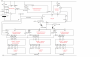
Good start. The 555 in use will charge and discharge the capacitor through the two resistors in place. There is a formula available to determine the charge, and discharge rate.
The 555's output is determined based on the charge/discharge rate previously which is pretty close to half second on, half second off. This will provide a 1Hz output signal from the 555 which is the basis for 'timing' everything on the board.
I am currently unsure where the 1000Hz signal source is though. Can you take a picture of the bottom?
The decade counters merely change their output every time they receive a clock pulse, but they are cascaded together, so one must reach 10 before the next will change.
They change the output of half a byte of data (4, bits) to represent 0 - 9
0000
0001
0010
0011
0100
0101
...
1001
These 4 bits are input to the 7 segment decoders which will output the proper combination to represent the number on the 7 segment display.
You also have an 74ls74 which is used to control the set/rest portion of the circuit. This chip is a 'pair' of flip flops. It can almost be seen as two chips packed in one.
I can write up some more details later. In the mean time, I encourage you to google for the ICs that are on that board. The resulting data sheets will tell you what each pin does. It will also occasionally show you the internal workings of the IC to help get a better understanding of how it works.
Thanks so much for your help already.
Let me first give my reply a title for reference later:
Post Title: 555 Internal components.
This post if 555 internal components part (i)
555 internal components part (ii) will come soon after.
I have printed out the data sheets and had a glance through them already I will go off and look at them in more detail now. I saw the internal workings in the datasheet before and they looked like trigger is at the (-) terminal of what I assume is a comparator, an even bigger assumption I will make now is that a comparator is a box that compares two independent voltage levels and depending on what it sees then it gives a dependent output. This goes into a box 'F/F'.
***Just a short note: I have come back after finishing this post to put in a piece of information, that is more relevant at this stage) regarding the "Trigger" comparator; The voltage at the + terminal of the "Trigger" comparator is Vcc(1/3)
The 'F/F' box:
This has an input from the trigger terminal (T).
- There is also an input connected to the emmiter terminal of a BJT, I am assuming NPN) with the collector of this BJT connected to discharge (7).
- The is an input from another Comparators output. This comparator is comparing the voltage levels at Control voltage (-), which is dictated to by (2/3)Vcc (assuming R=R=R, i.e. Resistros are equal ohms) and Threshold (+).
- There is an 'Output Stage' box between F/F and the output terminal, I do not know what this does or if it does anything (Apart of course from our approx 50/50 1Hz duty cycle wave).
- There is another terminal to the F/F box and this is connected to Reset (4) through the collector of an PNP BJT, the emmiter is at some voltage reference, in my circuit I think is at some level whereby the 555 never resets because the base and collector are always in Reverse Bias because the Base (N region) of this BJT is connected to Reset (4) input which is constantly held at +5V.
The Flip Flop is starting to look like the beating heart of the 555 IC.
*** Assuming 'F/F' stands for FlipFlop, and if I remember back to my theory on JK flip flops that;
- If J and K are both 0, the output does not change.
- If K is 1 and J is 0 then the output goes to 0.
- If J is 1 and K is 0 then the output goes to 1.
- If both J and K are both 1 then the output toggles between 0 and 1.
[Again this is assuming for now that these are not D-Type or some other type of Flip Flop that I don't know about.]
So continuing on with all these assumptions (i just trying to figure it out as I go);
Zooming back out to the higher level of abstraction, the 555 timer as a box, if you will. We spoke about how we can charge and discharge the capacitor earlier. This is effectively putting;
- Threshold (6) and Trigger (2) at either 5V or 0V,
- Discharge (7) at either (5V)(1/10) = 0.5V when C1 is S/C i.e uncharged OR 0V when C1 is O/C i.e. charged.
- +Vs (8) is always connected to 5V.
- And 'Reset' is always connected to +5V.
- Terminal 1 is always connected to ground.
- Output (3) is where over output voltage levels come out, High or Low.