Maker Pro
Maker Pro

Having trouble analyzing this power supply..

electronika.design

Feb 25, 2016
9
Joined
Feb 25, 2016
Messages
9
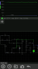
This is a power supply circuit I found while working on a project. I have been trying to analyse it but I am not getting the point of using Zener2 & Zener 3 in the circuit.
If anybody comes to know what it acts like or can relate it to something you already know, please send me a response.
Thank you.
 

Attachments

  • Power Supply ckt.PNG
    Power Supply ckt.PNG
    33.9 KB · Views: 176

AnalogKid

Jun 10, 2015
2,892
Joined
Jun 10, 2015
Messages
2,892
Your schematic ius very poor, and makes it impossible to answer your question.

2N0000 is not a valid part number. Diodes generally start with 1N.., and 1N0000 is not a valid part number.
33 mf means 33,000 microfarads. Is this really what you mean?
What are the voltage ratings for zener2 and zener3?
Are you sure zener2 and zener3 are drawn correctly?
What is the transistor part number?

The way the schematic is drawn, the b1 circuit is a 6 mA constant current load on the supply output.

ak
 

cjdelphi

Oct 26, 2011
1,166
Joined
Oct 26, 2011
Messages
1,166
I recreated your circuit, added what i thought was missing, this will give you a nice cleanish 5v output...

But please don't use it if you have to come in contact with it daily, when the 240v cap on input fails, your heart will fail as well if you're touching anything conductive
 

Attachments

  • Screenshot_2016-02-26-01-28-36.png
    Screenshot_2016-02-26-01-28-36.png
    183.9 KB · Views: 130

electronika.design

Feb 25, 2016
9
Joined
Feb 25, 2016
Messages
9
2N0000 is a general name given for diodes..plz ignore it
and its an NPN transistor
this is a similar one using transformer...plz go through this one too.
thank you
 

Attachments

  • Power Supply ckt.PNG
    Power Supply ckt.PNG
    29.7 KB · Views: 125

AnalogKid

Jun 10, 2015
2,892
Joined
Jun 10, 2015
Messages
2,892
Again, what are the values of the two unmarked zener diodes, and are you sure they are installed the way you want them?
Again, what is the exact value of the capacitor marked 33 mf? mf is not a valid electronic component abbreviation.

ak
 

electronika.design

Feb 25, 2016
9
Joined
Feb 25, 2016
Messages
9
Again, what are the values of the two unmarked zener diodes, and are you sure they are installed the way you want them?
Again, what is the exact value of the capacitor marked 33 mf? mf is not a valid electronic component abbreviation.

ak
According to me the Zener 2 & 3 diodes are used in forward biased connection. Yes! they are installed the same way as here.
and the value of capacitor is 33 micro farad/400v.
 

electronika.design

Feb 25, 2016
9
Joined
Feb 25, 2016
Messages
9
I recreated your circuit, added what i thought was missing, this will give you a nice cleanish 5v output...

But please don't use it if you have to come in contact with it daily, when the 240v cap on input fails, your heart will fail as well if you're touching anything conductive
Thnx...What software are you using for the analysis
 

AnalogKid

Jun 10, 2015
2,892
Joined
Jun 10, 2015
Messages
2,892
Z2 and Z3, as conventional forward-biased diodes, combine with the transistor's base-emitter junction and the emitter resistor (100 ohms) to form a 6 mA current sink circuit. This presents a minimum load on the power supply even when there is nothing attached externally. The output of the power supply is a full-wave rectified sine wave of 160 V peak (in the US), clipped to a max value of 24 V by D1. So it is a mostly DC output that pulses down to 0 V twice per input cycle. With no external load, power dissipation in zener diode D1 is over 15 W at 120 VAC input. That's a lot, and this is a very poor design.

ak

Edit: 7 mA current sink.
 
Last edited:

electronika.design

Feb 25, 2016
9
Joined
Feb 25, 2016
Messages
9
Z2 and Z3, as conventional forward-biased diodes, combine with the transistor's base-emitter junction and the emitter resistor (100 ohms) to form a 6 mA current sink circuit. This presents a minimum load on the power supply even when there is nothing attached externally. The output of the power supply is a full-wave rectified sine wave of 160 V peak (in the US), clipped to a max value of 24 V by D1. So it is a mostly DC output that pulses down to 0 V twice per input cycle. With no external load, power dissipation in zener diode D1 is over 15 W at 120 VAC input. That's a lot, and this is a very poor design.

ak
While im trying to analyze the ckt, I checked voltage across emitter register 100 ohm which turns out to be 0.7volt and at the base of transistor 1.280volt and at the VCE is 23.20 volts (PEAK value).
this means that transistor is not turning on....am i right???
 
Top