Sorry for not giving you the credit for it
")
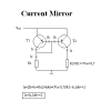
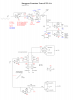
It's not my circuit. And having a schematic is a lot better than a description in text.
Main thing is that you're being given the same advice. And you've noticed that
I could almost not believe it so I tried shorting the Re:s back and forth but it stayed stable at 7%.
Do you mind if I don't try explaining that?
And I think it even does not need to be that complicated (omitting the strange Iref resistor and Q1).
Rref/Iref (or similar) is very important in that it generates a convenient (and low) reference voltage.
Because, please tell me if I'm wrong, U+=U- (while the OP is working)
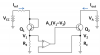
It will do while the conditions are such that the op-amp can force it to be the case. This essentially means until the voltage and/or current demanded/required of the output exceed chat the op-amp is capable of. The simple example is where the output would have to exceed Vcc. Also note that the inputs may have limits as to what voltages are permitted. If one is allowed to exceed that range, it may be that the op-amp stops doing what is required to get the other one there.
Basically, as long as you are operating within the specs, and the negative feedback loop exists, and you don't require an output the op-amp is not capable of, yes, the two inputs will track each other very closely (and can typically be said to have the same voltage)
which means that V2 will be equal to V1 at "all" times (i.e regardless of strange behaviour of Vbe2).
Well, not at all times... But when the circuit is operating correctly.
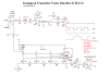
This means that Iout=Vcc/Re2 (where I have denoted Re2 as being the rightmost resistor).
Let's call the leftmost current source Iref, and the leftmost resistor Rref. Now let's call the rightmost resistor Rx and the current Ix
The voltages at both inputs will be the same, so Iref*Rref = Ix*Rx
Rearranging that, we get Ix = Iref.(Rref/Rx)
So the important thing is the ratio of the resistances to the reference current. The resistances allow you to multiply the reference by an arbitrary amount.
Now, there are practical considerations.
1) You want the loss across the resistor Rx to be small (to both minimise dissipation, but also to allow the output to get closer to ground -- I'll explain why that is important later)
2) You want to ensure that the inputs of the op-amp remain within allowable limits. Assuming you are not using a split supply for the op-amp, it needs to be one which operates with both inputs close to (or at) ground potential.
3) You need to ensure that the output does not need to exceed Vcc (or whatever the maximum output voltage is)
All these lead to Rx needing to be a low voltage, typically dropping around 0.1V to 0.7V at full load.
Because the input IRef and Rref effectively just generate a voltage Vref, there is no reason not to use a voltage source here. You might use a precision regulator (with a voltage divider to get the required voltage) or you might simply use a voltage divider from your supply voltage (assuming it is sufficiently stable).
Because Vref = Iref*Rref, the new equation for Ix is Ix = Vref/Rx
What the op-amp does (essentially) is modulate the base current to ensure that the current through the transistor is this calculated value.
The base voltage will hovver around Ix*Rx + 0.7V. The current supplied will be approximately Ix/G, where G is the gain of the transistor.
What you need to do is to ensure that the output of the op-amp is capable if the maximum voltage/current demand. If, for example, the voltage across the resistor rose so far that the output voltage would need to exceed Vcc (or the op-amp's supply voltage if they are different) then current regulation will be lost (and incidentally the two inputs would not be at the same potential)
Quite often the voltage source from which the current is drawn will be higher than the op-amp's supply voltage to allow the impedance of the load to vary more widely. However this also means a greater dissipation in Q1
Mission accomplished
You always need to be sure not to say this until it is actually true.