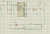
It does in this circuit, but in a way probably not intended: optocoupler=on -> MOSFET ) off.
I think that the intention is optocoupler=on -> MOSFET=on is what
@emrebay wants (is that so?) . That would be the fail-safe setup as the MOSFET will be off whenever it is not actively turned on.
Think of the optocoupler (or photocoupler
@(*steve*) is that an AE vs. BE thing?) as a switch. You'll want to switch BAT4's positive voltage to the gate of the MOSFET. Your circuit does that but only when the optocoupler is off. In that case BAT4 voltage is divided by R2, R3 and R4 which is really not necessary and will slow down the MOSFET as the gate capacitance is charged rather slowly.
A play of thought to get you started:
- Remove R2, R3 and R4 and replace the optocoupler by a switch to control Q1 by BAT4. Then you should immediately see how the optocoupler needs to be connected to Q1. This is your turn-on circuit.
- Now you will need a resistor to limit inrush current from BAT4 to Q1's gate. Your choice of 10 Ω is not bad. Where will you place it?
- Next consider the MOSFET's gate charge when the optocoupler is turned off. This charge will keep the MOSFET on when it should be off. A well placed resistor can discharge the Gate to BAT4's negative pole.
From this verbal description you should be able to construct the circuit. I'll have to leave the design of the schematic to you. You can upload it for us to check it.
That's what I told you in post
#7. Why haven't you then separated them? You're still using the same gnd for all parts of the circuit. Note that this is not necessarily wrong when done correctly, but can lead to confusion where current flow is possible in this circuit. I suggest you remove gnd from the isolated part of the circuit (right side of U2 and connected components) completely. It is not required here.