Maker Pro
Maker Pro

Buck Converter Calculations - Halp!

Raven Luni

Oct 15, 2011
798
Joined
Oct 15, 2011
Messages
798
Greetings,

Total brain fart on this one. I bought a bench supply for higher current projects (5-15V, up to 15A). One of the things I want to do is charge my ultracapacitors which are rated for 2.7V. A buck converter would seem like the way to do it but I'm tripping over the maths and the numbers are trying to eat me :eek:

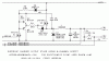
There are a few design limitations mainly due to the components I have available. IRF520 is the only power MOSFET I have so everything's designed around that - taking 10V as the input, using a 555 for the PWM (with chosen values it should have roughly a 25% duty cycle @ 33.2kHz). I'd like to deliver about 5A but not sure if the diode will hold up This is what I have for a design so far.

buck1.gif

I have no idea how to calculate the values for the inductor. I will need to wind my own but the equations for doing this make me cry :p I know its best to avoid saturation and fully charging the thing so can I get away with just throwing on alot of turns and hoping for the best? I'll need fairly thick wire too I'm guessing?

I was also wondering about current limiting resistors. Even if I set the current limit at the supply wont the voltage drop out initially since a discharged capacitor looks like a short (or is that where the inductor comes in)? If I was to use resistors to limit current then 10V @ 5A = 50W and I dont have anything that can take that (most ive got is some 7W resistors).

Anyway - any help or even radically different suggestions much appreciated :)
 

BobK

Jan 5, 2010
7,682
Joined
Jan 5, 2010
Messages
7,682
First of all, you need a P-channel MOSFET in that circuit. Then I think you can just drive the gate from the '555. You don't need the 2200uF since it is just going to be in parallel with your supercap.

Basically think of it not as a voltage regulator, think of it as loading up some current into the inductor, then dumping that current into capacitor.

You have to choose an inductor that can handle the current without saturating. Then you cal calculate how much time it will take to load the current into the inductor via

dI/dt = V / L

For example, a 1mH inductor with 10V across it will gain 10000 amps per second or 1amp in 100us.

Oh, and you have to stop it when the capacitor reaches the desired voltage.

Bob
 

KrisBlueNZ

Sadly passed away in 2015
Nov 28, 2011
8,393
Joined
Nov 28, 2011
Messages
8,393
As BobK suggests, you should use a P-channel MOSFET, with drain and source reversed (source connected to the incoming supply positive rail).

Alternatively you can use an N-channel MOSFET if you provide a suitable gate drive waveform. As it stands, using an N-channel MOSFET, the design won't properly turn on the MOSFET. The MOSFET needs its gate to be 5~10V higher than its source, to properly saturate. But when it is saturated, it pulls its source up to its drain voltage (i.e. the input supply voltage), so the gate voltage needs to be 5~10V higher than that. MOSFET gate driver ICs are available to produce a suitable drive signal, normally using a capacitor/diode charge pump to generate the higher positive voltage. Also it's wise to connect a zener between gate and source to prevent damage, and a series resistor in the gate signal.

Also a 1N4001 is totally unsuitable as the recovery diode - it's much too slow. Usually you'd use a Schottky diode such as the 1N5819 (1A maximum current, like the 1N4001) or something meatier. If you want 5A out of the power supply, you need a diode rated for at least 5A.

Of course, you could just buy one of those Chinese buck regulator boards based on a National Semiconductor part, and save yourself a lot of trouble!

If you're charging supercaps from it, you're going to need current limiting. Actually I'd suggest using a current regulator - your whole circuit should be designed to provide up to 5A at up to 2.7V. You can detect the supercap current using a series resistor with a transistor base-emitter junction across it, and reducing the output voltage while the transistor conducts. That wastes a significant amount of energy in the shunt, though. A Hall effect current sensor might be a better idea. The output voltage (the duty cycle) should be reduced by either VOUT > 2.7V OR IOUT > 5A so both parameters are limited simultaneously.

You're not going to be able to make anything usable with just a few bits you have lying around. You're going to have to fight your inclination to be canny, and oil those hinges on your wallet! But it's worth it - there are some amazing components available nowadays. Have a look at datasheets on Digikey or Mouser. Some of them are pure techno-porn! Texas Instruments, Maxim, Linear Technology...
 
Last edited:

BobK

Jan 5, 2010
7,682
Joined
Jan 5, 2010
Messages
7,682
Hi Luni,

Here is a circuit I designed for a constant current LED booklight. This circuit is designed to provide 30ma across the LED and actually was able to do so as the 9V battery ran down all the way to 4V. For 5A you would need to beef up the power components, (inductor, mosfet and shottky diode). The circuit works as follows. At turn on there is no current and the comparator is off, turning on the MOSFET. The current builds thorugh the inductor until the current sense resistor is higher than the reference (simple diode drop in this case). Then the comparator flips and turns off the MOSFET. When the current fall again enough to go below the comparator hysterisis, the cycle begins again. The neat thing is that it is all current controlled, the duty cycle and frequency automatically adjust to the load, which is just what you need in charging a supercap.

Hope this gives you a start.

Bob
 

Attachments

  • booklight.JPG
    booklight.JPG
    34.5 KB · Views: 861

Raven Luni

Oct 15, 2011
798
Joined
Oct 15, 2011
Messages
798
Ok based on some of the suggestions, it occurs to me that I could be looking at the wrong end of the problem. The goal is to charge a capacitor to a desired voltage. The only requirement is that the voltage across the capacitor does not exceed a certain level (which I've chosen to be 2.5V). The supply itself is already current limited and I've chosen a limit of 5A. Does it actually matter how many volts are used to charge the capacitor as long as it is switched off when it reaches the threshold?
 

KrisBlueNZ

Sadly passed away in 2015
Nov 28, 2011
8,393
Joined
Nov 28, 2011
Messages
8,393
The supply itself is already current limited and I've chosen a limit of 5A.
Do you mean that the supply you're feeding into your charger circuit has a 5A current limit? If so, that's not a workable way to do things. If your circuit pulls too much current, the power supply will limit by dropping the output voltage, and your circuit will no longer work properly. You need to detect the output current being fed into the supercap and limit it by altering the behaviour of your circuit.
Does it actually matter how many volts are used to charge the capacitor as long as it is switched off when it reaches the threshold?
That's not really a meaningful sentence. If you mean does the input voltage to the charger matter, no it doesn't, you're right. I was talking about the output voltage from your charger, which is equal to the voltage across the supercap. This voltage starts at zero when the supercap is fully discharged. As you feed current into the supercap, this voltage rises, at a rate calculated by dv/dt = I/C. In other words, for a fixed capacitance, the higher the current, the faster the voltage will rise, as you'd expect. Obviously you need to detect the voltage limit being reached, and stop charging at that point. Until that voltage is reached, you need to regulate the duty cycle of your switching converter to give the desired charging current.
 

BobK

Jan 5, 2010
7,682
Joined
Jan 5, 2010
Messages
7,682
Kris,

I think Raven was suggesting that he just use a constant current supply and no buck converter. This should work, although I would question how well it would work when the capacitor was near zero. But it will waste a lot of power by lowering the output voltage with a resitive (or shunt) element. The beauty of the buck converter is that the current is limited by indutance with no power loss (well, a much smaller power loss anyway).

Bob
 

Raven Luni

Oct 15, 2011
798
Joined
Oct 15, 2011
Messages
798
As it stands, using an N-channel MOSFET, the design won't properly turn on the MOSFET. The MOSFET needs its gate to be 5~10V higher than its source, to properly saturate. But when it is saturated, it pulls its source up to its drain voltage (i.e. the input supply voltage), so the gate voltage needs to be 5~10V higher than that. MOSFET gate driver ICs are available to produce a suitable drive signal, normally using a capacitor/diode charge pump to generate the higher positive voltage.

So your're saying that if drain-source voltage is 10V then the gate would have to be 15-20V? That doesnt make sense. Anyway I understand why a P channel would be better there - and if I use an N channel with the output on teh drain side this should be equivalent yes?

The purpose of the 2N3904 in my circuit was to deliver 10v @ approx. 160mA to the gate which should be enough to switch it. Shouldn't just be a matter of moving the load to the other side of the MOSFET and finding a suitable replacement for the diode (and of course getting the right inductor).
 

KrisBlueNZ

Sadly passed away in 2015
Nov 28, 2011
8,393
Joined
Nov 28, 2011
Messages
8,393
I think Raven was suggesting that he just use a constant current supply and no buck converter.
His schematic shows a switching converter and he hasn't mentioned a linear regulator. As you say, a linear regulator is always an option but it wastes power. He could use a switching pre-regulator and a linear regulator for the last few volts, but at 5A he would still be wasting and dissipating a fair bit of power.

BTW I like your "book light" design. I simulated it and it seems to work pretty well. I like the idea of using the inductor's characteristics to control the frequency by determining when the MOSFET is turned off.

So your're saying that if drain-source voltage is 10V then the gate would have to be 15-20V? That doesnt make sense.
Right, it doesn't! An N-channel MOSFET is turned on by a positive gate-source voltage of, let's say, 5V and saturated by, say, 10V. If your circuit has the MOSFET's drain connected to a positive supply, and you apply 10V to the gate with the source as the output, the MOSFET will turn on, and will pull its source upwards towards the supply rail. As this happens, the gate-source voltage drops - effectively it pulls the rug out from underneath itself. The MOSFET will settle at a point in its linear region where the gate-source bias is high enough to sustain the source current.

To properly drive an N-channel MOSFET in your configuration, you need to make sure that the gate is 10V more positive than the source WHEN the MOSFET is conducting, at which time its source voltage is (nearly) equal to its drain voltage, which is the positive supply. That's why you need a higher rail - called a "boost" function in switching converters that use N-channel MOSFETs (many National Semiconductor devices).

Anyway I understand why a P channel would be better there - and if I use an N channel with the output on teh drain side this should be equivalent yes?
No, you can't take the output from the drain in that topology. If you ground the source, so you can use a ground-referenced 0V/10V swing on the gate, then the drain switches to ground, not to the positive supply rail.

The purpose of the 2N3904 in my circuit was to deliver 10v @ approx. 160mA to the gate which should be enough to switch it.
The 555 can do that. At least, the bipolar versions are rated to source and sink 200 mA. The low power versions like the TLC555, TS555 etc aren't, though.
 

Raven Luni

Oct 15, 2011
798
Joined
Oct 15, 2011
Messages
798
Ah - now I get it. I originally bought those MOSFETs for experimenting with class D amplifiers (which I have still to get round to) so I'm guessing the same priciples will apply there as well (the job there will be fast switching).

I'll have to read up on gate drivers (I always thought they were mostly for impedance matching of amplifier outputs)
 

Raven Luni

Oct 15, 2011
798
Joined
Oct 15, 2011
Messages
798
Ok - been looking into this again - specifically bootstrapping. I found this in a forum. The poster seems to have nicked it from somewhere and didnt say (so if its one of yours speak up :p )

Anyway, would this be suitable for my purposes and if so, how would I choose the right capacitor based on the switching frequency?

bootstrap.png
 

KrisBlueNZ

Sadly passed away in 2015
Nov 28, 2011
8,393
Joined
Nov 28, 2011
Messages
8,393
Here's my suggestion for an output stage for your supercap charger. It's a combination of the bootstrapped drive circuit you found, and a standard buck regulator with load current sensing. I've added a buffer stage and some protection components.

I suggest you build it and play around with it. Use a resistor load initially, and don't draw more than, say, 1A. I haven't shown the control circuitry. Initially you can use a 555 but I think you'll have to get more complicated than that. You might be best to use a switching regulator control chip or the Linear Technology device I've linked to at the bottom of the post.
attachment.php


Here's how it works. The control signal controls Q1, which inverts it. Q1's drain is buffered by Q2 and Q3 which form a low-impedance buffer to provide strong drive to MOSFET Q4, which is essential to ensure fast switching and therefore low power dissipation. DP limits the MOSFET's gate-source voltage to prevent damage.

Assume that initially the drive signal is high, so Q1's drain is low, so Q4 is OFF and its source is at 0V. The VB node is at about 11.6V because of DB. When the drive input goes low and Q1 turns off, its drain is pulled up to VB by RP and this causes Q2 to conduct and supply current into Q4's gate. As Q4 starts to conduct, its source voltage rises, and this voltage rise is coupled onto VB by CB, causing VB to rise as well. This in turn enables Q2 to provide more gate voltage to Q4, which causes its source to rise more, and so on.

This trick of using the MOSFET's own output signal to boost its own drive voltage is called bootstrapping, as you know. It relies on the fact that the MOSFET is being switched ON and OFF continuously. It cannot keep the MOSFET saturated steadily forever because CB will eventually discharge and the gate voltage will start to drop. While the circuit is switching, CB's charge is topped up by current through DB and RB. The value of CB is not critical; I've suggested 1 uF (I would use a good quality capacitor, none of this multi-layer ceramic rubbish :) and that will be fine for any switching frequency over 1 kHz.

The output stage is a standard buck regulator. When Q4 is ON, current in L increases, and when Q4 is OFF, DC (commutation diode) conducts and keeps the current flowing as the current in L decreases. The mean current through L is equal to the load current.

The output voltage is smoothed by CS which should probably be a low-ESR component. Check the ripple current specification; you may need two or more in parallel. The capacitance is not very important. RL provides a minimum load to ensure that Q4's ON-time doesn't become extremely short. (This is only relevant when you have closed the regulation loops.) RS detects the load current and is needed if you want to regulate the output voltage and current simultaneously. The value specified will give 0.6V drop at 6A.

The inductor is a complicated subject. It's been a while since I did any design of custom inductors, and that was only using RM-type ferrite cores. There are formulas but there's also a lot of experimentation needed.

I tried to work everything out for you, but I've given up. I'm just not confident that I know what I'm doing now. I picked a switching frequency of 75 kHz, and estimated the inductance at about 10 uH, which sounds pretty low to me.

You could just look on Digikey or Mouser or whoever for a pre-wound inductor that can handle a peak current of around 40% more than your maximum continuous output current, i.e. 8.4A or more, and has an inductance of around 10 uH, or get several inductors between 10 uH and 100 uH, and do some experimenting.

Those are the critical parameters: the inductance and the saturation current.

Don't try to draw a lot of current out of it initially. If possible, monitor the inductor current with an oscilloscope and increase the load gradually, while you watch for saturation (the inductor current suddenly starts to go up quickly). If the inductor saturates, you could easily destroy the MOSFET.

You should also check that the gate drive waveform to the MOSFET is nice and clean through the switching region (the area between 2V and VCC+8V).

Sorry I can't be more use. It's a while since I did this stuff and I don't have my notes. (They're at the company where I used to work.) Here are some documents and sites that I looked at while trying to work it all out, that could be useful or interesting:

http://info.ee.surrey.ac.uk/Workshop/advice/coils/gap/index.html
http://www.linear.com/product/LTC3608
http://diysmps.com
http://www.poweresim.com/index2.jsp?topologytype=5
http://www.micrometals.com/
 

Attachments

  • RAVEN1.001.GIF
    RAVEN1.001.GIF
    5.1 KB · Views: 5,376

Raven Luni

Oct 15, 2011
798
Joined
Oct 15, 2011
Messages
798
Thats excellnt. Thankyou very much :)
I feel obliged to do something nice in return now :)
 

KrisBlueNZ

Sadly passed away in 2015
Nov 28, 2011
8,393
Joined
Nov 28, 2011
Messages
8,393
You're welcome.
I would be interested to hear the results of your experimentation. Please continue to post on this thread.
Kris
 

Raven Luni

Oct 15, 2011
798
Joined
Oct 15, 2011
Messages
798
Will do. I got myself a raspberry pi recently so maybe I can use that for the control and sensing :)
 

KrisBlueNZ

Sadly passed away in 2015
Nov 28, 2011
8,393
Joined
Nov 28, 2011
Messages
8,393
Yes, maybe. Does it have onboard ADC and DAC features?

I would love to get a Raspberry Pi too, and I probably will someday.
 

Raven Luni

Oct 15, 2011
798
Joined
Oct 15, 2011
Messages
798
Not sure yet - havent had much time to play with it yet.
In other news, I've been harvesting components from that crappy bench supply I bought and there is a PWM controller board based around a TL494 as well a a couple of nice big inductors and other components plus that nice meter display module (posted a pic of that in the frankenstein thread). I will see if I can reverse engineer a schematic from the board (what a fun mini project).
 

Raven Luni

Oct 15, 2011
798
Joined
Oct 15, 2011
Messages
798
Ok - here's as much as I could decipher from that PWM board. It's not very tidy - its just from following the traces on the board and fitting stuff in as I went. The 2 diodes marked ??? are black bodied but I couldnt make out the markings.

pwm.jpg
 

Raven Luni

Oct 15, 2011
798
Joined
Oct 15, 2011
Messages
798
Oh well I think I'll bin that one - far too much meaningless information reading up on the tl494. That was clearly a chip designed by wankers for wankers ;)
 
Top