Maker Pro
Maker Pro

7 Transistors Triangle Wave Generator (650Khz)

iimagine

Oct 23, 2013
55
Joined
Oct 23, 2013
Messages
55
Google Triangle Wave Generator and almost all that you get are circuits that employ 2 comparator/opamp ect...
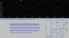
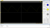
Well I wanted an alternative, more efficient way of doing this, so I designed this circuit in LTSpice. It simulates well, giving a very nice, highly linear waveform. uses very little power! The only problem is that I dont have a lab (I only have a breadboard and a DMM). I'm asking for help on test this out and to prove that it works. Any comment or suggestion is much appreciated.

I'm planning on using this for my Discrete Class D Amp

Thanks in advance

PS: If any one need to understand how this works, I can explain in detail.
 

Attachments

  • DTO_650Khz.PNG
    DTO_650Khz.PNG
    46.3 KB · Views: 1,294

KrisBlueNZ

Sadly passed away in 2015
Nov 28, 2011
8,393
Joined
Nov 28, 2011
Messages
8,393
That looks like a nifty little circuit!

How will you get the thermal tracking for the current mirror transistors if you use discrete components?

Would you consider tidying up the schematic by adding wires so the components don't touch so closely?

I would like to see a circuit description, yes.
 

iimagine

Oct 23, 2013
55
Joined
Oct 23, 2013
Messages
55
That looks like a nifty little circuit!

How will you get the thermal tracking for the current mirror transistors if you use discrete components?

Would you consider tidying up the schematic by adding wires so the components don't touch so closely?

I would like to see a circuit description, yes.

For thermal tracking, I was thinking of expoxy them together.

Given a voltage ref of 2.5V via R3/R4 divider (can be adjusted if a different amplitude is desired) Q5 starts to turn on, providing a path for Q1 toward ground, current mirror Q2 starts to conduct and charge the capacitor C1. When C1 reaches 2.5V Q6 starts to turn on because now its base voltage is higher then its emitter. Q6 'steals' Q5's base current, cutting it off, shutting down current mirror Q1/ Q2. C1 discharges into Q6 base, keeping it on until its voltage drops down to R1/R2 threshold, at which point Q7 sees a diff between its base and emitter voltage, and starts to turn on, cutting off Q6. When Q6 is cutoff its no longer 'steals' current from Q5 base, so Q5 begins to turns on and the cycle repeats.
 

KrisBlueNZ

Sadly passed away in 2015
Nov 28, 2011
8,393
Joined
Nov 28, 2011
Messages
8,393
Nice! Thanks for the explanation. I can follow it but I don't think I have a complete and natural understanding of it yet.

I simulated it, and got good results. This will allow me to explore it further, if I have the time and inclination to :)

Would it be better to use a transistor array for thermal tracking? Or perhaps some dual transistors? Digikey have a large range in SMT packages.

Also, why did you use a different transistor for Q5~7?
 

iimagine

Oct 23, 2013
55
Joined
Oct 23, 2013
Messages
55
Would it be better to use a transistor array for thermal tracking? Or perhaps some dual transistors? Digikey have a large range in SMT packages.

Also, why did you use a different transistor for Q5~7?

Yes, It is definitely better to use transistor array, or dual transistors!

Q5-7 are high speed, high freq transistors. We are talking about 600Khz+ freq here :D. You can replace these with any fast Ft and low junction capacitance transistors. These are generally in RF and UHF range.
 

KrisBlueNZ

Sadly passed away in 2015
Nov 28, 2011
8,393
Joined
Nov 28, 2011
Messages
8,393
Isn't it also important to use high-frequency transistors for Q1~4?
 

iimagine

Oct 23, 2013
55
Joined
Oct 23, 2013
Messages
55
Isn't it also important to use high-frequency transistors for Q1~4?

Q3/Q4 are being used to sink current, not switching so these can be any general purpose NPN
Q1/Q2 has been suggested by other to be replaced by hi-freq ones but in simulation I did not notice any diff so I left them alone. It would be better to use hi-freq ones though
 

KrisBlueNZ

Sadly passed away in 2015
Nov 28, 2011
8,393
Joined
Nov 28, 2011
Messages
8,393
Q4's collector voltage isn't constant, so I guess its function isn't simply static - its Miller capacitance at least will be relevant. I tried changing Q3 and Q4 to 2N2369s in the simulation and the emitter node waveform squares up slightly, but you're probably right that it's not worth worrying about. The cleanness of the emitter voltage isn't really important I guess; it's the change in currents in the transistors that needs to be quick and clean, right?

As for the PNPs, I see what you mean - the whole current sink is being turned on and off so their frequency response would be more important, but I didn't think LTSpice knew about any really high-frequency PNPs. Which ones did you try?
 

iimagine

Oct 23, 2013
55
Joined
Oct 23, 2013
Messages
55
more efficient version

Got rid of 1 current mirror, saving more power and less headache from bjt matching :D!
Added an extra current source for more linearity :)
 

Attachments

  • DTO_2.PNG
    DTO_2.PNG
    50.8 KB · Views: 386

KrisBlueNZ

Sadly passed away in 2015
Nov 28, 2011
8,393
Joined
Nov 28, 2011
Messages
8,393
I'm impressed!

I had a lot of trouble understanding your first circuit until I redrew it in a way that shows the logical progression of the signals. I also rewrote the description. I'm posting it here in case you want to do a similar re-layout of your new design.

I haven't changed anything apart from replacing R2 with a diode. I don't know whether that's a good idea or not; I just did it that way because it makes it more obvious that the circuit is there to provide a fixed voltage on Q7's base. I also changed the capacitor to slow things down and reduce the effects of charge storage in the transistors - at 800 kHz the emitter waveform looks quite different from how it looks with a 33 nF capacitor.

attachment.php


I've had a good play around with the circuit and I think I understand it pretty well now. Thanks for sharing it!

Edit: There's an error in the description. The third line of the first paragraph mentions a voltage of 3.6V. This related to an experiment (removing R4 to reduce component count) and is not correct for the diagram shown.
 

Attachments

  • triangle.gif
    triangle.gif
    22.4 KB · Views: 1,181
Last edited:

iimagine

Oct 23, 2013
55
Joined
Oct 23, 2013
Messages
55
I'm impressed!

I had a lot of trouble understanding your first circuit until I redrew it in a way that shows the logical progression of the signals. I also rewrote the description. I'm posting it here in case you want to do a similar re-layout of your new design.

I haven't changed anything apart from replacing R2 with a diode. I don't know whether that's a good idea or not; I just did it that way because it makes it more obvious that the circuit is there to provide a fixed voltage on Q7's base. I also changed the capacitor to slow things down and reduce the effects of charge storage in the transistors - at 800 kHz the emitter waveform looks quite different from how it looks with a 33 nF capacitor.

I've had a good play around with the circuit and I think I understand it pretty well now. Thanks for sharing it!

First of all, I thank you for your interest and supports this little circuit of mine.

Replacing R2 with a diode will limits the bottom peak of the signal to ~1.2V instead of ~0.8V, other than that, it is fine.

Now that you have had a good playing around with it, will you test it out in real world? :D I dont have an oscilloscope :(

Edit: Scratched that comment about Q3/Q4 bandwidth.
 
Last edited:

iimagine

Oct 23, 2013
55
Joined
Oct 23, 2013
Messages
55
Well, my hantek6022BE PC based oscilloscope arrived! I went right ahead to test the circuit, using:
Q1/Q2 = MPSA93 Matched hfe to ~7
Q3/Q4 = 2n3904 Matched hfe to ~7
Q5/Q6 = MPSA42 Matched hfe to ~7
Q7 = 2n3904
R1/R2 = 100k/10k
R3 = 470k
No R4, I wanted top peak at ~5v
C1 = 1nF

It does oscillate! :D However the waveform is unexpected :confused: I will investigate this at a later time
Any suggestion or comment is appreciated
Edit: Using my first circuit
 

Attachments

  • DTO_Realworld_1.jpg
    DTO_Realworld_1.jpg
    81.5 KB · Views: 306
Last edited:

KrisBlueNZ

Sadly passed away in 2015
Nov 28, 2011
8,393
Joined
Nov 28, 2011
Messages
8,393
I can't promise that I will build the circuit. I'm interested in it, but probably not THAT interested! I'm glad that you've built it up.

Interesting that the waveform is wrong. I'm sure you understand the design better than I do, but I have a few suggestions for you to consider.

1. Use a Darlington emitter follower to buffer the capacitor voltage.
2. Try using a larger capacitor value (in case the problem is related to the high frequency)
3. Get some dual transistors for the current mirrors.
4. Try lower values for R3.

Have you simulated the circuit with R3=470k? I tried a few different values for R3 when I was experimenting with removing R4 and the value seemed to be important. Why did you set it so high?

I don't know what you mean by "Matched hfe to ~7".

Do you think it's worth building up your second design?
 

iimagine

Oct 23, 2013
55
Joined
Oct 23, 2013
Messages
55
Have you simulated the circuit with R3=470k? I tried a few different values for R3 when I was experimenting with removing R4 and the value seemed to be important. Why did you set it so high?

I don't know what you mean by "Matched hfe to ~7".

Do you think it's worth building up your second design?

If you look at the falling slope, it is not linear. This is caused by R3 being too low, causing Q6's collector to take in more current, more Ic means less Ib, therefore the non linearity and dragging time.

What I meant by 'Matched hfe to 7' was that the hfe of both transistors were measured to be around 7 in different

Now what really confused me is the at the peak, It seems that Q6 is not triggered on fast enough

I'll continue to test this out, if all else fail, i'll go to the second circuit :)

If I could only find the time
 

iimagine

Oct 23, 2013
55
Joined
Oct 23, 2013
Messages
55
Introducing R4 to the prototype got rid of the flat line

R3/R4 = 470k/470k

Freq is now around 8kHz

Only one problem left, the rising slope early effect
 

Attachments

  • DTO_Realworld_2.PNG
    DTO_Realworld_2.PNG
    51.6 KB · Views: 279

(*steve*)

¡sǝpodᴉʇuɐ ǝɥʇ ɹɐǝɥd
Moderator
Jan 21, 2010
25,510
Joined
Jan 21, 2010
Messages
25,510
Monitor the voltage across the capacitor.

My guess is that the constant current used to either charge or discharge it is not really constant.

I've not been following this closely enough to know if the rising edge of the output waveform occurs during charge or discharge of the capacitor.
 

iimagine

Oct 23, 2013
55
Joined
Oct 23, 2013
Messages
55
Since I cannot solve that problem, I've come up with another circuit. This one is even simpler, symmetry can be adjusted via R5 (RSense); square wave can be seen at Q1's collector (much better than the previous version). The working principle is the same only the discharging method is changed

I'm going to test this one soon, hopefully it will work

I will learn not to trust LTSpice from now on :)
 

Attachments

  • DTO_3.PNG
    DTO_3.PNG
    70.6 KB · Views: 306

KrisBlueNZ

Sadly passed away in 2015
Nov 28, 2011
8,393
Joined
Nov 28, 2011
Messages
8,393
This one is pretty straightforward. I've redrawn it so its operation is clear.

attachment.php


You can see that the charge current is not constant, and that will cause distortion in your class D amplifier. Also the symmetry depends on the gain of the charge transistor which will vary with temperature, but the symmetry should not be important in your application.

I haven't tried it at high frequencies.

I'm interested in this apparent failure of LTSpice to properly predict your first circuit's operation. Is it possible there is a good reason for that? Perhaps breadboard capacitance? Loading effect of the oscilloscope? Some other real-world factor?
 

Attachments

  • tri-v3.gif
    tri-v3.gif
    18.7 KB · Views: 968

CDRIVE

Hauling 10' pipe on a Trek Shift3
May 8, 2012
4,960
Joined
May 8, 2012
Messages
4,960
I will learn not to trust LTSpice from now on :)

I wouldn't be so quick to dismiss your LT Spice results. It's far more likely that the discrepancies lie elsewhere as Kris stated. What's the input resistance/cap of your scope? Are you using a low cap 10X probe. What's the scope coupling - AC/DC? If your using a 10x probe did you adjust the compensation cap before using it? Is your scope a USB model or one of those far less desirable audio input models which are very low BW and AC coupling only. They'll also load the hell out of anything connected to it with both R, C & L.

I'm interested in this apparent failure of LTSpice to properly predict your first circuit's operation. Is it possible there is a good reason for that? Perhaps breadboard capacitance? Loading effect of the oscilloscope? Some other real-world factor?

Kris, reproducing the loading effect of his scope should be easy enough in spice but reproducing all the stray C found on a protoboard would be ..uh..EEEEK! :eek::D

Hey, this is one of those moments that great ideas are born from. Think about this for a moment... My Tina will convert any schematic (.sch) to a 3D view that's layed out on a protoboard. Would it not be totally cool to be able to plug in the row/column count of a given protoboard (including unused rails) and have the software calculate all the stray capacitances over the entire grid? Click another button to insert all of the stray capacitance (as Hidden or click to View) and your good to go. I would also imagine that software could also analyze the jumpers too.

I think I'm musing again. :p
Chris
 
Top