Maker Pro
Maker Pro

4 Channel Diversity Controller

wakesetters

Jun 13, 2013
3
Joined
Jun 13, 2013
Messages
3
Hey, just joined this forum.

I am into First Person View (FPV) radio control planes and I have been putting together this project for awhile. I am still new to circuit board electronics and would love some input/feedback on this project.

Basically the idea is to have 4 video recievers using their (RSSI) outputs, build a controller that will select the best signal...

Now i have seen multiple designs on other forums but none that i can find on a diagram with 4 channels.


As can be seen in my diagram the inputs go into a 4 channel comparator chip (LM339). My question is this: 'The negative inputs to the comparator chip, should they be bridged together like this? Will this mean that the highest voltage will be selected from the 4 channels?

diversitycontrollerscot.jpg


Thanks in advance , wakesetters
 
Last edited:

KrisBlueNZ

Sadly passed away in 2015
Nov 28, 2011
8,393
Joined
Nov 28, 2011
Messages
8,393
Hi wakesetters and welcome to the electronics point forums :)

That's an interesting problem. No, the circuit you have won't do what you want. There's nothing wrong with tying all the inverting inputs of the quad comparator together; the problem is that there's nothing driving them, so they will just float and pick up noise.

I have some ideas for how to do what you want, but they need work, so I will think about them and get back to you.

In the meantime... You mentioned you've seen circuits that do this with only two inputs; could you post links to some of them please?

Also, is there an issue with video synchronisation? If the cameras aren't synchronised, switching the video signal from one to another will cause the display device to "hiccup" as it loses then regains frame sync. Some TVs might even blank the display for a short time. You don't want the display to black out every time the camera view changes!

One more thing. The RSSI outputs from your receivers. I assume the voltage increases with increased received signal strength, is that right?

Edit: Also, what are the minimum and maximum voltages for the RSSI signals coming out of the receivers?
 
Last edited:

KrisBlueNZ

Sadly passed away in 2015
Nov 28, 2011
8,393
Joined
Nov 28, 2011
Messages
8,393
Another question. Why do you want this function? Are the transmitters all on different frequencies so they suffer from fading under different circumstances? Or are the receivers at different locations? I can't think of any other reason why you would need four independent radio paths from the plane to the same point on the ground.

Edit: Oh I get it. There's one signal from the plane, received by four receivers in different places, and sent to a common monitoring point, right?
 
Last edited:

wakesetters

Jun 13, 2013
3
Joined
Jun 13, 2013
Messages
3
Thanks KrisBlue for the warm welcome!

Here's a link to the forum that has helped me the most.

http://www.rcgroups.com/forums/showthread.php?t=1169075

Take particular attention to "version #2" as i have based my design around this way of thinking. He provides two schematics one that is for positive scaling RSSI controllers & another that is for inverse scaling. As for the RSSI outputs from my receivers I have yet to test them. I brought home my multimeter from work today, so I shall test this over the weekend.

To clarify a little more on the project, I am running four 1.2Ghz Receivers. There is one 1.2Ghz transmitter on-board the plane transmitting back live video feed. All Receivers are set to the exact same channel. The only difference is that i will be using different antennas on each receiver. One receiver will be using a Skew planar antenna which will give out a circular coverage for a km or so... The rest will be using Yagi antennas for super long range. Yagi antennas are directional and provide a coverage of around 30 degrees but at long distances.

So in layman's terms by using 3 Yagi's i can have super long coverage of about 90 degree's but i also have a skew planar as a backup in-case the plane fly's behind me.

This might explain better...

60se.jpg


You made a great point with video signal switching... it would be very annoying if everytime the channel switched, the screen blanks out!!! I was thinking maybe i could add a capacitor in the circuit somewhere to back feed signal to the video output when the switch is made... but yer i 'm not sure.

"Edit: Oh I get it. There's one signal from the plane, received by four receivers in different places, and sent to a common monitoring point, right?" - Yes, not really different places but more so different antennas :)
 
Last edited:

KrisBlueNZ

Sadly passed away in 2015
Nov 28, 2011
8,393
Joined
Nov 28, 2011
Messages
8,393
I get it. I've been thinking about how best to do this. I'm still thinking. I'll get back to you within a few days.

Regarding video switching. If all the receivers are receiving exactly the same signal, then a quick change between them shouldn't cause a problem. Ideally it would be best if changes could be synchronised with a change of frame. I'll think about that. It is all getting a bit complicated.

I will check out your link in a few days. Thanks for the link. I'm otherwise occupied (at my partner's place) for the next three days or so.

KrisBlueNZ
 

KrisBlueNZ

Sadly passed away in 2015
Nov 28, 2011
8,393
Joined
Nov 28, 2011
Messages
8,393
OK, I've come up with a few design ideas. In this post I'll cover the two essential parts of the design: the highest RSSI detector and the video signal switcher.

The whole circuit is designed to operate from a +12V supply. The video switcher IC needs a regulated voltage so I have used a 78L08 regulator there.

attachment.php


This diagram shows an instantaneous highest RSSI detector. It accepts four RSSI voltages (RSSI0~RSSI3) and produces four outputs (IHR0~IHR3). Each output is high (+12V) if the corresponding RSSI input has the highest voltage, otherwise it is low.

The RSSI outputs from the receivers must always be in the range +1V to +7V and a higher voltage is considered to mean a higher received signal strength. A wide RSSI voltage range is good because it means that input offset voltages in the op-amps will contribute less error.

Outputs are not guaranteed to be exclusive. It is possible for two (or even more) outputs to be active simultaneously, if two or more RSSI voltages are very close together. It is also possible for all outputs to be simultaneously low, though this should only happen for very short time intervals - a few microseconds at a time.

The circuit contains four identical sections, one for each RSSI input. They are connected together by a node called IHR, which represents the instantaneous highest RSSI voltage, and has a pull-down resistor RIHR.

Each circuit monitors the IHR voltage, and is able to drive it positive by enabling its MOSFET. The IHR node becomes an analogue "OR" of the four RSSI voltages.

Within each section of the circuit, the op-amp compares the incoming RSSI voltage against the IHR voltage. If the RSSI voltage is lower than IHR, the op-amp's output will go low, and the BS107 MOSFET will turn OFF because it has no gate bias. The 1N914 diode completes the feedback loop to keep the op-amp in linear mode.

If the incoming RSSI voltage rises above the IHR voltage, the op-amp's output voltage will increase, and this will turn on the MOSFET, feeding current into IHR. This current increases until IHR reaches the incoming RSSI voltage, then it stabilises. The IHR voltage is now equal to the incoming RSSI voltage. The current that is feeding the IHR rail comes through the MOSFET's drain resistor; provided that there is at least 0.7V across RIHR, this current will be enough to forward-bias the BC557B PNP transistor, which will pull the IHRn output high.

The circuit block which had previously been driving IHR will stop driving IHR because IHR is now higher than its incoming RSSI voltage. No current will flow through its MOSFET, and its PNP transistor will receive no bias, so its IHRn output will fall low.

attachment.php


This is the video switcher circuit. This uses a MAX4545 RF/video switching circuit that contains four switches. One switch at a time is enabled, to feed the appropriate video signal through to the output.

The MAX4545 is designed to run from power supplies up to 12V but it can be damaged by voltage spikes on the power supply, so I have chosen to use a 78L08 regulator to provide a +8V supply for it. The 0V/12V logic signals that control the switches need to be dropped down to 0V/8V; this is done with four voltage dividers.

The video feeds from the four receivers come in on nets named VID0~VID3 (corresponding to RSSI0~RSSI3). These signals must be positive relative to the 0V rail; this is normal for composite video. If the signal goes negative, the MAX4545 could be damaged. I suggest you use a socket for it!

The video switches inside the MAX4545 are all connected to a common node called VIDOUT; this is the signal for the display monitor.


This design is not complete. There are two significant issues:

1. The highest RSSI detector circuit may produce two or more output signals simultaneously. If two or more video switches were enabled simultaneously, no damage is likely to occur, but the video signals might interfere with each other.

2. The switching between different video signals can occur at any time. This could cause disturbances to the display. I think the changes should be synchronised to the vertical blanking time, which happens once per field in the video signal (60 times per second for NTSC, 50 times per second for PAL and SECAM).

I have designed a priority circuit that will eliminate the problem of having two or more signals selected simultaneously, and I am working on the vertical retrace synchronisation. This extra circuitry will consist of several CMOS ICs and some small components. I will post again in a few days.

Please let me know what you think of the design. Would you be comfortable building it?
 

Attachments

  • Rssi1.gif
    Rssi1.gif
    11 KB · Views: 1,881
  • Rssi2.gif
    Rssi2.gif
    6.8 KB · Views: 2,304

KrisBlueNZ

Sadly passed away in 2015
Nov 28, 2011
8,393
Joined
Nov 28, 2011
Messages
8,393
What video standard are you using?
 

KrisBlueNZ

Sadly passed away in 2015
Nov 28, 2011
8,393
Joined
Nov 28, 2011
Messages
8,393
Full schematic

OK, here's the full schematic of my suggested design.

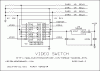
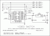
I'm reposting the first two blocks (the highest RSSI detector and the video switcher) because I've made some small changes to them. The circuit description in my earlier post still applies.

attachment.php


attachment.php


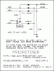
Here are the remaining three sections of the design.

attachment.php


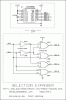
The prioritiser deals with the problem of multiple "highest RSSI" outputs being on simultaneously. It converts the four signals from the highest RSSI detector module (actually, it only needs three of them) into a two-bit binary number that represents the number of one of the highest RSSI receivers.

The behaviour of the outputs in relation to the inputs is described in text on the diagram. The upshot is that the number represented by the output bits is always a receiver that has a highest RSSI indication, except during startup when the highest RSSI has not yet been determined.

You can draw up a truth table for the sixteen combinations of the four inputs, and check that the outputs are correct for every possible combination.

attachment.php


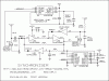
This module is the synchroniser. It detects vertical synchronisation pulses in the selected video signal and latches the two-bit binary receiver number in a CD4013 dual flip-flop. This number is only allowed to change during vertical retrace, and periodically if the sync separator stops detecting sync. (This would happen if the transmitter fails, for example, and no receivers can produce a valid video signal.)

Here is a simplified circuit description.

U4 is an LM1881N application-specific linear IC that is designed to extract sync information from a composite video signal in either NTSC, PAL or SECAM format. It receives its signal from VIDOUT, the chosen receiver signal. It generates a short low pulse on its VSYNC output during each vertical sync pulse. During this time, there is no video displayed on the monitor, so it is safe to change receivers without disturbing the picture.

The LM1881 can operate from a 12V supply but 8V is plenty and there is an 8V rail available, so I chose to use that.

U5D and U5E are connected as a latch. This latch controls the discharge of CFT (field timeout capacitor) and the clocking of U6, the selection latch. Normally U5E's output, and U5D's input, are low. The field timeout capacitor and related circuitry are used so that if the vertical sync pulses from U4 cease, due to loss of the signal, the circuit will continue to clock U6 periodically. If it didn't do this, the last selected receiver would remain selected indefinitely, regardless of any new RSSI information.

The start of each vertical sync pulse causes a positive transition on QVS's drain; this is coupled through the capacitor and diode into U5D's input and sets the latch. This turns on QFT, which discharges CFT, resetting the field timeout. After about 100 us, the capacitor on U5C's input reaches U5C's input threshold, and U5C's output goes low and pulls U5D's input low, turning off the latch. So in response to each vertical sync pulse, QFT is turned on for about 100 us, long enough to fully discharge CFT.

In between sync pulses, CFT charges up through RFT. If pulses stop, after a delay of at least 20 ms (typically 25~35 ms) (longer than the longest possible field time), U5F's output goes low, pulling U5E's input low and setting the latch again, causing a new pulse on U6's clock inputs.

U6 is a clocked latch. On every rising edge on its clock inputs (pins 3 and 11) it samples the levels on HRB0 and HRB1, the two bits from the prioritiser that identify the receiver with the highest RSSI. The latch outputs are SB0 and SB1, which feed the selection expander.

attachment.php


The selection expander expands a two-bit binary number (SB0 and SB1) into four indivual active-high selection signals for the four video switches in the MAX4545 in the video switcher block.

I have shown two alternative circuits. U7 is a CD4555B or HCF4555B dual two-to-four decoder with active high outputs; it is perfect for this application, but it is not widely available. I had never heard of it until I looked for a CMOS 4000-series device that would do this particular function. It is probably very little-used and will probably be on "pending discontinuation" lists, so it may not be wise to design it in.

The alternative circuit uses the two remaining spare gates in U5, and another IC, to perform the same function. These ICs are still fairly widely used. The four NOR gates from U8 each respond to a different combination of the two-bit binary number, and drive their outputs high (to enable the appropriate video switch) only when that binary number matches the combination they have been wired for.

If you use the CD4555 option, you must connect the inputs of the two unused gates in U5 to the ground or +12V rail (it doesn't matter which), otherwise they will float and pick up noise, which can cause problems.


As you see, I have assumed that your video feed is NTSC, PAL or SECAM. If that's not the case, I will need more information about the video signal. The LM1881 sync separator has some flexibility - the RSET resistor can be changed to accommodate different vertical sync intervals.

If you decide this project is too difficult, don't worry. I've enjoyed designing it, and the design (or parts of it) may be useful to other people.

Important note. I have not tested any of this design! If you go ahead with it, please send me a PM so we can keep in touch during the testing phase.
 

Attachments

  • RSSICOMP.A.002.GIF
    RSSICOMP.A.002.GIF
    11.3 KB · Views: 1,659
  • RSSICOMP.B.002.GIF
    RSSICOMP.B.002.GIF
    7.1 KB · Views: 1,643
  • RSSICOMP.C.002.GIF
    RSSICOMP.C.002.GIF
    5 KB · Views: 1,435
  • RSSICOMP.D.001.GIF
    RSSICOMP.D.001.GIF
    9.7 KB · Views: 1,694
  • RSSICOMP.E.001.GIF
    RSSICOMP.E.001.GIF
    8.2 KB · Views: 1,532

wakesetters

Jun 13, 2013
3
Joined
Jun 13, 2013
Messages
3
Thanks KrisBlue, for your the time that you have put into helping this project. Much appreciated.

Since my last post i have been asking others on what they also think of this project. I have since changed my plans from logic to coding with an arduino board. This has made the project a lot complex.

Using simple coding and a lot less wires i have been able to reconfigure this project and so far in testing it is working quite nicely.

Thanks again

-Scott
 

paulpaulo26

Sep 16, 2014
3
Joined
Sep 16, 2014
Messages
3
Dear scott,

can you contact me directly by email , i want to speak with you about the same project like yours a "4 rssi diversity" for fpv.

thank you

[email removed]
 
Last edited by a moderator:

KrisBlueNZ

Sadly passed away in 2015
Nov 28, 2011
8,393
Joined
Nov 28, 2011
Messages
8,393
Hi paulpaulo26 and welcome to Electronics Point.

I have removed the email address from your post for your own safety. If Scott still uses Electronics Point, he can respond to you using a private message.

This thread is over a year old so you may not get a response from him.
 

paulpaulo26

Sep 16, 2014
3
Joined
Sep 16, 2014
Messages
3
hi KrisBlueNZ,

do you have his email ? can you tell him ?

i search him because i have the same project , 4 comtech diversitty based rssi signal. Work with arduinoà, but i dont know arduino !

i have picture and composant list to make it but the problem is just the arduino code to change the comtech rx with the best rssi signal .

Do you know where can i find the explication ?

thank you very much

paul from fance
 

KrisBlueNZ

Sadly passed away in 2015
Nov 28, 2011
8,393
Joined
Nov 28, 2011
Messages
8,393
Hi Paul. No, I don't know him. I don't know about the application either. I will send you a PM with the email address he used to register on Electronics Point.
 
Top