Well, I've had a go at designing something. The circuit simulates OK but it's pretty large. Also I don't know whether it would comply with any electrical requirements - in your area, or anywhere else.
I've drawn it up in LTSpice. I don't have models for the high-voltage transistors I specified; I used generic LTSpice transistor models called 2N5401 (for the PNPs) and 2N5550 (for the NPNs). I used NPNs for both current sources because at high voltage and significant power dissipation, NPNs have much better performance.
I'm posting it here just for interest's sake. I DO NOT make ANY claims about this design.
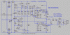
Here's a circuit description.
The LED light bulb is shown at the right, starting from Cin. The LED light bulb responds to current of either polarity. The higher the current, the brighter the LED will light. Also, the higher the current, the more rapidly the input capacitor (Cin, 1.6 uF) in the bulb will charge or discharge, and the more rapidly the voltage across the bulb will change. The circuit generates alternating positive and negative currents into the bulb. These currents are supplied by "Darlington-and-a-half" transistors QP1/2/3 and QN1/2/3
Starting from the left of the schematic, the AC mains voltage (230V RMS nominal) is rectified by D1~4 and smoothed by C1, and becomes the main positive rail (across the top of the diagram). The voltage on this rail, measured relative to the 0V rail (along the bottom of the diagram) is nominally about 324V and the design maximum is 400V.
C1's value should be 2 uF multiplied by the LED current (in mA) at the maximum brightness setting, in order to keep the ripple on the main positive rail to less than about 5V peak to peak. Ripple doesn't affect the circuit much; you could use 1 uF per mA for C1 to save space or cost.
The circuit comprised of DD1, DD2, DS1, DS2, RD and DS3 sets up several voltages, relative to the positive and negative rails. DD1/DD2 and DS1 set the voltages at both ends of the "brightness" trimpot, which is shown here as two resistors, POTA and POTB. These voltages are about 1.4V and 7.6V negative relative to the positive rail.
DS2 adds another 15V to create a voltage reference about 23V below the positive rail, which is used by QL1, described later. RD drops the bulk of the voltage and sets the current in that path to about 1 mA. DS3 sets another reference voltage at about 15V above the 0V rail, which is used by QL2, also described later.
The "Darlington-and-a-half" transistors formed by triplets QP1/2/3 and QN1/2/3 have a relatively high current gain (I have assumed at least 2000 total beta for each compound transistor) and can withstand 400V DC. Almost all of the power is dissipated in the final transistor of the triplet, which is specified as a BUX85G and dissipates on average about 60 mW for each mA of LED bulb current. For example, operating at an LED current of 50 mA, QP3 and QN3 will dissipate about 3W each.
The current limiters are identical and use a simple, standard design, which is documented at
http://en.wikipedia.org/wiki/Constant_current_source
The current is controlled by current from the collectors of QPS and QNS. This current develops a proportional voltage across RPB or RNB, and the emitter follower action of the QP1/2/3 triplet ensures that the voltage across RPE or RNE follows. DP1~3 or DN1~3 provide compensation for the three base-emitter drops in the transistors. The result is that the collector-emitter current is limited to a value which is roughly equal to the current from QPS (for the top current source) multiplied by RPB divided by RPE.
QPS and QNS are also adjustable current sources. They provide the current that controls QP1~3 and QN1~3 respectively. Only one is enabled at a time; this is ensured by DPS and DNS, which are driven by QFF1 and QFF2, only one of which is ON at a time. When the appropriate QFFx transistor is ON, the appropriate QxS transistor is enabled as a current source with its current controlled by the voltage at the bases of QPS and QNS, which is set by the Brightness potentiometer.
In this diagram, the Brightness potentiometer is represented by resistors POTA and POTB, which are calculated according to the pot_position parameter in the simulation, which represents the position of the Brightness potentiometer in percent, in the range 0~100. This produces values for POTA and POTB which add to 100 kilohms, the resistance of the Brightness potentiometer in a real (not simulated) circuit.
The feedback loop is completed by the flip-flop made from QFF1 and QFF2. The outputs of the flip-flop, on the collectors of those transistors, control the QPS and QNS current sources, which in turn control the two large current sources that supply the output.
The flip-flop is set and reset when the voltage at the output point gets closer to the positive or negative supply rail than the "limit" reference voltages set by DS1~3. When the output voltage goes higher than the voltage at DS2 anode, which is roughly equal to the positive supply rail minus 22V, QL1 conducts and forces QFF1 ON, forcing QFF2 OFF. When the output voltage goes lower than the voltage at DS3 cathode, which is roughly 15V higher than the 0V rail, QL2 conducts, causing QL3 to conduct and turning on QFF2, forcing QFF1 OFF.
The circuit alternates between these two states, with the output connection slewing alternately positive and negative at a rate determined by the current provided by the active current source (positive and negative currents are roughly equal) and the load capacitance, which mainly consists of Cin in the LED light bulb. The current that flows through Cin also flows through the LED(s) in the light bulb.
The actual LED bulb current that corresponds to the maximum brightness setting is determined by the values of RPE and RNE. The value of these resistors is chosen according to the formula R = 5.7 / ILED(max).
The voltage applied across the LED lamp is about 270V peak to peak and unipolar. In the real world running from AC mains the LED would see about 650V peak to peak, bipolar.
The waveforms show the current into the LED bulb at five different settings of the Brightness potentiometer:
0% (pink)
25% (cyan)
50% (red)
75% (blue)
100% (green)
Comments anyone?