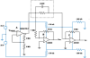
This is an ill-conceived circuit.
Clearly the load is high impedance, hence the attempt to "measure" the load voltage without "loading" by using op-amp B with an inverting input configuration and a 1 MΩ input resistor. This in conjunction with a 10 kΩ feedback resistor, yields a gain of 10,000 / 1,000,000 = 1 / 100 = 0.01. So even with a 35 V output from op-amp A, the output of op-amp B will be limited to 0.35 volts. So far, so good. But why is the 1 MΩ resistor even necessary?
The load is being driven by a low-impedance source, the output of op-amp A, so a simple voltage divider consisting of a 100 kΩ and 1 kΩ resistor in series between the load and common will produce a voltage across the 1 kΩ resistor approximately 0.01 times the input voltage. This can be applied to the non-inverting input of op-amp B, and the output of op-amp B would be connected to the inverting input to implement a unity-gain buffer with high input impedance. The reduction in resistance value will lower the Johnson noise injected into this buffer circuit by the 5 MΩ resistor. The AS820 is a good choice for this part of the circuit.
However, although the load may be high impedance, it is driven from the low-impedance output of op-amp A configured as a G = 2 non-inverting buffer. The 5 MΩ resistors are much too large for this task. Lowering their values will reduce the noise contributed by op-amp A. The ADA4700-1 is capable of 30 mA output, so resistors more on the order of 10 kΩ passing 35 / 20,000 = 1.75 mA would be appropriate. The high-voltage capability of the ADA4700-1 is a good match for this part of the circuit.
Op-amp C has its inverting input connected to the "ground" side of the load and its non-inverting input is grounded. That means the "ground" side of the load is connected to a "virtual ground" by means of the 5 MΩ feedback resistor. The voltage output of op-amp C will be the load current multiplied by 5,000,000. So a two microampere load current will result in a 10 V output from op-amp C. The low bias current presented by the AD549 makes it a good fit for this application because of the large feedback resistor and presumably large source impedance of the load.
The voltage divider resistors used at the positive and negative rails of op-amps B and C are not by-passed. If this circuit configuration is to be used, 10 μF to 100 μF capacitors should be installed between both rails and common. In addition, 0.1 μF capacitors should be installed between the op-amp power rail terminals and common, as close as possible to those terminals. This is a "fix a bad design" band-aid solution. You should install three-terminal voltage regulators to bring the ±35 V supplies down to ±15 V.
")
